SLUSAD7B April 2011 – July 2016 UCC25710
PRODUCTION DATA.
- 1 Features
- 2 Applications
- 3 Description
- 4 Revision History
- 5 Description (continued)
- 6 Pin Configuration and Functions
- 7 Specifications
- 8 Detailed Description
-
9 Application and Implementation
- 9.1 Application Information
- 9.2
Typical Application
- 9.2.1 Design Requirements
- 9.2.2
Detailed Design Procedure
- 9.2.2.1 Determining Transformer and Resonant Circuit Parameters
- 9.2.2.2 CS (Output Current Sense)
- 9.2.2.3 ICOMP (Current Amplifier Compensation)
- 9.2.2.4 SS (Soft Start)
- 9.2.2.5 FMAX (Maximum VCO Frequency)
- 9.2.2.6 FMIN (Minimum VCO Frequency)
- 9.2.2.7 GD1 and GD2 (Gate Drive 1 and 2)
- 9.2.2.8 LEDSW (LED Switch Drive)
- 9.2.2.9 DSR (Dimming Slew Rate)
- 9.2.2.10 DTY (Dimming Duty-Cycle Average)
- 9.2.2.11 DADJ (Dimming Duty-Cycle Adjust)
- 9.2.2.12 OV (Output Overvoltage)
- 9.2.2.13 UV (Output Undervoltage)
- 9.2.2.14 CL (Current Limit)
- 9.2.3 Application Curves
- 10Power Supply Recommendations
- 11Layout
- 12Device and Documentation Support
- 13Mechanical, Packaging, and Orderable Information
Package Options
Mechanical Data (Package|Pins)
- DW|20
Thermal pad, mechanical data (Package|Pins)
Orderable Information
7 Specifications
7.1 Absolute Maximum Ratings
over operating free-air temperature range (unless otherwise noted)(1)| MIN | MAX | UNIT | ||
|---|---|---|---|---|
| Supply voltage | VCC | 20 | V | |
| LEDSW output current | ILEDSW | ±2 | mA | |
| VREF output current | IVREF | –20 | ||
| Gate drive RMS current continuous GD1, GD2 | IGD1, IDG2 | 25 | ||
| Gate drive voltage, GD1 GD2 | VGD1, VGD2 | –0.5 | VCC + 0.5 | V |
| Voltage | CS, CL, OV, UV, BLON, DIM, CREF | –0.5 | 7 | |
| Lead temperature 1.60 mm (1/16 inch) from case for 10 s | 260 | °C | ||
| Operating junction temperature, TJ | –55 | 150 | ||
| Storage temperature, Tstg | –65 | 150 | ||
(1) Stresses beyond those listed under Absolute Maximum Ratings may cause permanent damage to the device. These are stress ratings only, which do not imply functional operation of the device at these or any other conditions beyond those indicated under Recommended Operating Conditions. Exposure to absolute-maximum-rated conditions for extended periods may affect device reliability.
7.2 ESD Ratings
| VALUE | UNIT | |||
|---|---|---|---|---|
| V(ESD) | Electrostatic discharge | Human-body model (HBM), per ANSI/ESDA/JEDEC JS-001(1) | ±2000 | V |
| Charged-device model (CDM), per JEDEC specification JESD22-C101(2) | ±500 | |||
(1) JEDEC document JEP155 states that 500-V HBM allows safe manufacturing with a standard ESD control process.
(2) JEDEC document JEP157 states that 250-V CDM allows safe manufacturing with a standard ESD control process.
7.3 Recommended Operating Conditions
all voltages are with respect to GND; currents are positive into and negative out of the specified terminal. -40°C < TJ = TA < 125°C (unless otherwise noted)| MIN | NOM | MAX | UNIT | ||
|---|---|---|---|---|---|
| VCC | Operating input voltage | 11 | 18 | V | |
| CVCC | VCC bypass capacitor | 0.47 | µF | ||
| Operating junction temperature | –40 | 125 | °C | ||
| Switching frequency at gate drive outputs | 25 | 350 | kHz | ||
| VCREF | Input voltage (linear range) | 0.6 | 1.65 | 2.7 | V |
| VCREF | Input voltage (using internal clamps) | 0 | VVREF | ||
| CVREF | VREF bypass capacitor | 0.22 | 1 | 2.2 | µF |
| CSS | SS capacitor | 10 | 250 | nF | |
| CICOMP | ICOMP capacitor | 0.5 | 47 | ||
| CDTY | DTY capacitor | 0.22 | 6.8 | µF | |
| CDSR | DSR capacitor | 0 | 2500 | pF | |
7.4 Thermal Information
| THERMAL METRIC(1) | UCC25710 | UNIT | |
|---|---|---|---|
| DW (SOIC) | |||
| 20 PINS | |||
| RθJA | Junction-to-ambient thermal resistance | 79 | °C/W |
| RθJC(top) | Junction-to-case (top) thermal resistance | 43 | °C/W |
| RθJB | Junction-to-board thermal resistance | 44 | °C/W |
| ψJT | Junction-to-top characterization parameter | 16 | °C/W |
| ψJB | Junction-to-board characterization parameter | 44 | °C/W |
| RθJC(bot) | Junction-to-case (bottom) thermal resistance | N/A | °C/W |
(1) For more information about traditional and new thermal metrics, see the Semiconductor and IC Package Thermal Metrics application report.
7.5 Electrical Characteristics
TA = –40°C to 125°C, TA = TJ, VVCC = 12 V, VBLON = 3 V, VUV = 3 V, VOV = 2 , VCL = 0 V, RMIN = 100 kΩ, RMAX = 4.99 kΩ, (unless otherwise noted)| PARAMETER | TEST CONDITIONS | MIN | TYP | MAX | UNIT | |
|---|---|---|---|---|---|---|
| SUPPLY INPUT | ||||||
| VVCCMAX | VCC operating voltage | 18 | V | |||
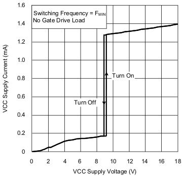
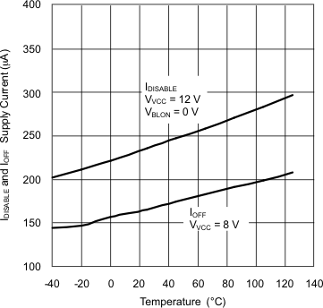
| IOFF | Supply current, off | VVCC = 8 V | 160 | 250 | µA | |
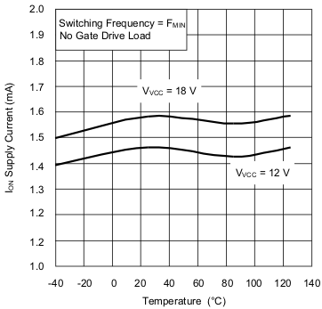
| ION | Supply current, on | Switching frequency = FMIN (30 KHz) | 1.4 | 2.1 | mA | |
| IDISABLE | Supply current, disabled | VVCC = 12 V, VBLON = 0 V | 240 | 350 | µA | |
| ILATCHOFF | Supply current, latched off | Fault latch set | 600 | 900 | ||
| UNDERVOLTAGE LOCKOUT | ||||||
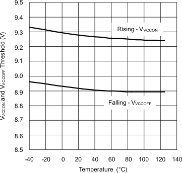
| VVCCON | VCC turnon threshold | VVCC low-to-high | 8.6 | 9.3 | 10.1 | V |
| VVCCOFF | VCC turnoff threshold | VVCC high-to-low | 8.3 | 9 | 9.6 | |
| VVCCHYS | Hysteresis | 0.2 | 0.35 | 0.5 | ||
| 5-V REFERENCE OUTPUT | ||||||
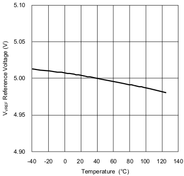
| VVREF | 5-V Reference | IVREF = 0 to 10 mA, TJ = 25°C | 4.95 | 5 | 5.05 | V |
| VVREF | 5-V Reference | IVREF = 0 to 10 mA, TJ = –40°C to 125°C | 4.85 | 5 | 5.15 | |
| CURRENT AMPLIFIER | ||||||
| VICOMPIOS | Input offset voltage | VCREF = 1.65 V, ICOMP tied to CS | –15 | 15 | mV | |
| ICS | Input bias current at CS input | VCREF = 1.65 V, VCS = 1.65 V | –0.25 | 0.25 | µA | |
| ICR | Input bias current at CREF input | VCREF = 1.65 V, VCS = 1.65 V | –0.25 | 0.25 | ||
| VICOMPHI | ICOMP high | VCS = 0 V, VCREF = 1.65 V, IICOMP = 50 µA | 4.6 | 4.85 | V | |
| VICOMPLO | ICOMP low | VCS = 3 V, VCREF = 1.65 V, IICOMP = –50 µA | 0.35 | 0.65 | ||
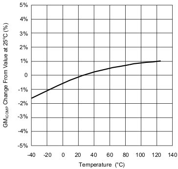
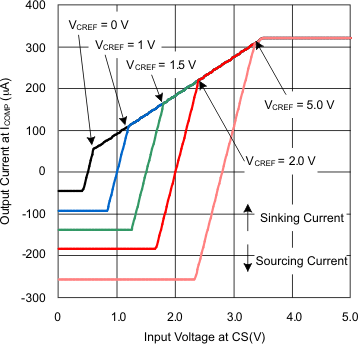
| GMICOMP | ICOMP transconductance | ICOMP tied to CS, IICOMP = –100 µA to 100 µA | 440 | 510 | 600 | µs |
| IICOMPSRC | Source current ICOMP | VCS = 0.65 V, VCREF = 1.65 V, VICOMP = 2.5 V | 120 | 150 | 180 | µA |
| IICOMPSNK | Sink current ICOMP | VCS = 2.65 V, VCREF = 1.65 V, VICOMP = 2.5 V | 195 | 245 | 295 | |
| IICOMPLGK | LED off leakage current at ICOMP | VDIM = 0 V, VICOMP = 2.5 V, TJ = –40°C to 85°C | –0.1 | 0.1 | ||
| VCREFCLO | CREF low Clamp | VCREF = 0 V, ICOMP tied to CS, regulating voltage at ICOMP | 0.475 | 0.5 | 0.535 | V |
| VCREFCHI | CREF high Clamp | VCREF = 3 V, ICOMP tied to CS, regulating voltage at ICOMP | 2.65 | 2.8 | 2.95 | |
| SOFT START | ||||||
| ISS | Soft-start charging current | VSS = 2.25 V | 2 | 2.5 | 3 | µA |
| RSSDC | Soft-start discharge resistance | VSS = 1 V | 3.4 | 5 | kΩ | |
| VSSTH | Soft-start threshold | SS clamp released | 3.95 | 4.15 | 4.4 | V |
| TRSTDLY | Reset delay | From UVLO turnon to start of soft start | 7 | 10 | 13 | ms |
| VOLTAGE CONTROLLED OSCILLATOR | ||||||
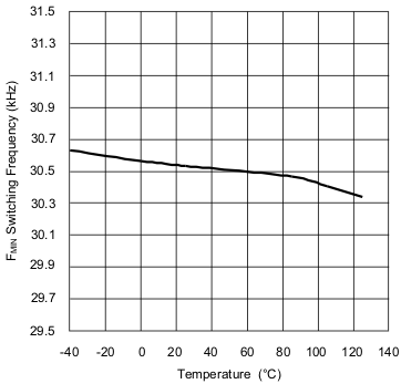
| FMIN | FMIN GD1, GD2 | RMIN = 100 kΩ, VICOMP = 5 V | 29.5 | 30.5 | 31.5 | kHz |
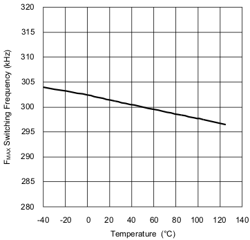
| FMAX | FMAX GD1, GD2 | RMIN = 100 kΩ, RMAX = 4.99 kΩ, VICOMP = 0.95 V | 275 | 300 | 320 | |
| TDT | Dead-time GD1, GD2 | RMIN = 100 kΩ, VICOMP = 3 V | 400 | 500 | 600 | ns |
| TMATCH | ON-time mismatching | RMIN = 100 kΩ, VICOMP = 3 V | –50 | 50 | ||
| VVCOTHLO | VICOMP VCO Threshold Low | Disable GD1, GD2, VICOMP high to low | 0.8 | 0.9 | 0.95 | V |
| VVCOMAX | VICOMP for FMIN | Frequency reaches FMIN | 3.8 | 4 | 4.2 | |
| GATE DRIVERS | ||||||
| VGDHI | GD1, GD2 VOUT high | IGD1, IGD2 = –20 mA, below VCC | 1.8 | 3 | V | |
| RGDHSRES | GD1, GD2 ON-resistance high | IGD1, IGD2 = –20 mA | 14 | 30 | Ω | |
| VGDLO | GD1, GD2 VOUT low | IGD1, IGD2 = 20 mA | 0.08 | 0.2 | V | |
| RGDLSRES | GD1, GD2 ON-resistance low | IGD1, IGD2 = 20 mA | 4 | 10 | Ω | |
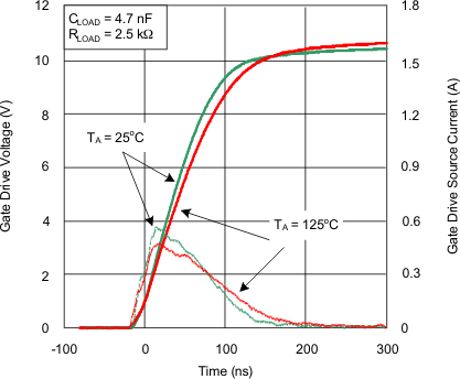
| TGDRISE | GD1, GD2 output rise time | CGD = 1 nF, 1 V to 9 V | 25 | 35 | ns | |
| TGDFALL | GD1, GD2 output fall time | CGD = 1 nF, 9 V to 1 V | 20 | 30 | ||
| UNDERVOLTAGE PROTECTION | ||||||
| VUVTH | Undervoltage threshold | High-to-low on UV input | 2.27 | 2.4 | 2.53 | V |
| VUVHY | Undervoltage threshold hysteresis | 190 | 240 | 300 | mV | |
| IUV | UV input bias current | VUV = 2.7 V | –0.25 | 0.25 | µA | |
| OVERVOLTAGE PROTECTION | ||||||
| VOVTH | Overvoltage threshold | Low-to-high on OV input | 2.46 | 2.6 | 2.74 | V |
| VOVHY | Overvoltage threshold hysteresis | 190 | 240 | 300 | mV | |
| IOV | OV input bias current | VOV = 2.3 V | –0.25 | 0.25 | µA | |
| CURRENT LIMIT PROTECTION | ||||||
| VCLTH | Current limit threshold | Low-to-high on CL input | 0.9 | 0.95 | 1 | V |
| VCLHY | Current limit threshold hysteresis | 375 | 475 | 525 | mV | |
| VCLLTH | Current limit latching threshold | Low-to-high on CL input | 1.75 | 1.9 | 2.05 | V |
| ICL | CL input bias current | VCL = 2.2 V | –0.25 | 0.25 | µA | |
| THERMAL SHUTDOWN | ||||||
| tTSD | Junction temperature at thermal shutdown | Temperature rising | 135 | 160 | 185 | °C |
| tHYS | Thermal hysteresis | 25 | 45 | |||
| BACKLIGHT ON INPUT | ||||||
| RBLON | RBLON pulldown resistance | Pull down to GND | 100 | 200 | 350 | kΩ |
| VBLON | Enable threshold | 0.8 | 1.2 | 1.6 | V | |
| PWM DIMMING | ||||||
| VDIM | Dimming input threshold | 1.2 | 1.5 | 1.8 | V | |
| RDIM | DIM pullup resistance | Pullup resistance to VREF, VDIM = 0 V – 4.5 V | 140 | 180 | 240 | kΩ |
| VLEDSWHI | High-level at LEDSW output | ILEDSW = –100 µA, below VCC, VDIM = 3 V | 0.4 | 1 | V | |
| VLEDSWLO | Low-level at LEDSW output | ILEDSW = 100 µA, VDIM = 0 V | 0.2 | 0.5 | ||
| RLEDSWHI | High-level output resistance | ILEDSW = –500 µA – 0 µA, VDIM = 3 V | 4 | 6 | kΩ | |
| RLEDSWLO | Low-level output resistance | ILEDSW = 500 µA – 0 µA, VDIM = 0 V | 2 | 3 | ||
| RDTY | DTY output resistance | VDTY = 0 V – 2.5 V , VDIM = 0 V | 30 | 40 | 50 | |
| VDTYH | DTY max level | VDIM = 0 V | 2.45 | 2.6 | 2.7 | V |
| VDTYL | DTY min level | VDIM = 3 V | 0.05 | 0.1 | 0.15 | |
| IDADJCH | DADJ charging current | VDADJ = 2.5 V, VDIM = 0 V | 16 | 20 | 25 | µA |
| RDADJDC | DADJ discharge resistance | VDADJ = 0.5 V, VDIM = 3 V | 1 | 1.5 | kΩ | |
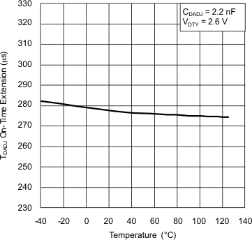
| TDADJ | DADJ delay | CADJ = 2.2 nF, VDTY = 2.6 V, delay from DIM high-to-low to DSR discharge | 225 | 275 | 330 | µs |
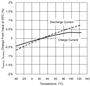
| IDSRCH | DSR slew rate charge current | VDSR = 2.5 V, VICOMP = 4 V, VDIM = 3 V | 38 | 44 | 50 | µA |
| IDSRDC | DSR slew rate discharge current | VDSR = 2.5 V, VICOMP = 4 V, VDIM = 0 V | 38 | 44 | 50 | |
| VDSRCL | DSR clamp above ICOMP | VICOMP = 2 V, level above VICOMP | 0.45 | 0.7 | 0.95 | V |
7.6 Typical Characteristics
