SLUS746D December 2006 – July 2024 UCC27200 , UCC27201
PRODUCTION DATA
- 1
- 1 Features
- 2 Applications
- 3 Description
- 4 Pin Configuration and Functions
- 5 Specifications
- 6 Detailed Description
- 7 Application and Implementation
- 8 Power Supply Recommendations
- 9 Layout
- 10Device and Documentation Support
- 11Revision History
- 12Mechanical, Packaging, and Orderable Information
Package Options
Mechanical Data (Package|Pins)
Thermal pad, mechanical data (Package|Pins)
Orderable Information
3 Description
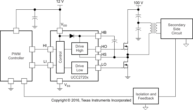
The UCC2720x family of high-frequency N-channel MOSFET drivers include a 120V bootstrap diode and high-side and low-side drivers with independent inputs for maximum control flexibility. This allows for N-channel MOSFET control in half-bridge, full-bridge, two-switch forward, and active clamp forward converters. The low-side and the high-side gate drivers are independently controlled and matched to 1ns between the turnon and turnoff of each other.
An on-chip bootstrap diode eliminates the external discrete diodes. Undervoltage lockout is provided for both the high-side and the low-side drivers forcing the outputs low if the drive voltage is below the specified threshold.
Two versions of the UCC2720x are offered. The UCC27200 has high noise immune CMOS input thresholds while the UCC27201 has TTL compatible thresholds.
| PART NUMBER | PACKAGE | BODY SIZE (NOM) |
|---|---|---|
| UCC2720x | D (SOIC, 8) | 3.9mm × 4.9mm |
| DDA (PowerPADTM SOIC, 8) | 3.9mm × 4.9mm | |
| DRM (VSON, 8) | 4.0mm × 4.0mm |
 Simplified Application
Diagram