SNVSAQ5B November   2018  – May 2022 UCC27282

PRODUCTION DATA  

  1. Features
  2. Applications
  3. Description
  4. Revision History
  5. Pin Configuration and Functions
  6. Specifications
    1. 6.1 Absolute Maximum Ratings
    2. 6.2 ESD Ratings
    3. 6.3 Recommended Operating Conditions
    4. 6.4 Thermal Information
    5. 6.5 Electrical Characteristics
    6. 6.6 Switching Characteristics
    7. 6.7 Timing Diagrams
    8. 6.8 Typical Characteristics
  7. Detailed Description
    1. 7.1 Overview
    2. 7.2 Functional Block Diagram
    3. 7.3 Feature Description
      1. 7.3.1 Enable
      2. 7.3.2 Start-up and UVLO
      3. 7.3.3 Input Stages and Interlock
      4. 7.3.4 Level Shifter
      5. 7.3.5 Output Stage
      6. 7.3.6 Negative Voltage Transients
    4. 7.4 Device Functional Modes
  8. Application and Implementation
    1. 8.1 Application Information
    2. 8.2 Typical Application
      1. 8.2.1 Design Requirements
      2. 8.2.2 Detailed Design Procedure
        1. 8.2.2.1 Select Bootstrap and VDD Capacitor
        2. 8.2.2.2 Estimate Driver Power Losses
        3. 8.2.2.3 Selecting External Gate Resistor
        4. 8.2.2.4 Delays and Pulse Width
        5. 8.2.2.5 External Bootstrap Diode
        6. 8.2.2.6 VDD and Input Filter
        7. 8.2.2.7 Transient Protection
      3. 8.2.3 Application Curves
  9. Power Supply Recommendations
  10. 10Layout
    1. 10.1 Layout Guidelines
    2. 10.2 Layout Example
  11. 11Device and Documentation Support
    1. 11.1 Device Support
      1. 11.1.1 Third-Party Products Disclaimer
    2. 11.2 Receiving Notification of Documentation Updates
    3. 11.3 Support Resources
    4. 11.4 Trademarks
    5. 11.5 Electrostatic Discharge Caution
    6. 11.6 Glossary
  12. 12Mechanical, Packaging, and Orderable Information

Package Options

Mechanical Data (Package|Pins)
Thermal pad, mechanical data (Package|Pins)
Orderable Information

Typical Characteristics

Unless otherwise specified VVDD=VHB = 12 V, VHS=VVSS = 0 V, No load on outputs
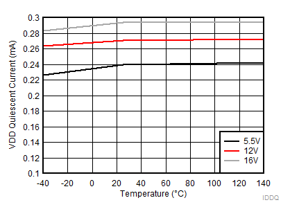
GUID-45CF0974-2393-4E70-9028-3F2E3D040EFA-low.gif
VHI = VLI = 0 V
Figure 6-1 VDD Quiescent Current
GUID-F5E39EDF-1C74-4673-9948-EDD753AC92E5-low.gif
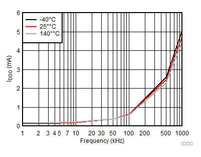
CL = 0 FVDD =VHB= 12V
Figure 6-3 VDD Operating Current
GUID-223F77ED-0FD4-484C-B0BE-B63321F370B0-low.gif
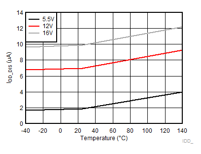
CL = 0 FVEN = 0 V
Figure 6-5 VDD Current When Disabled
GUID-D2DDD225-B3C0-4E88-B798-4B04EC4F4163-low.gif
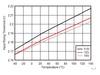
Figure 6-7 Input Rising Threshold
GUID-71E6224C-FCC2-41A0-A38E-63950FAB5798-low.gif
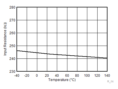
Figure 6-9 Input Pull-down Resistor
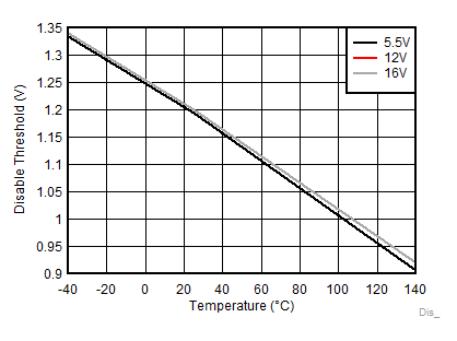
GUID-8B236B99-1205-4FFE-BF19-0DA2F2C66E23-low.gif
Figure 6-11 Disable Threshold
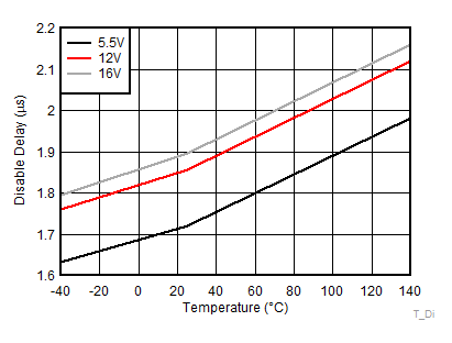
GUID-3652820C-D5AD-46B7-B61A-DABE027FC298-low.gif
Figure 6-13 Disable Delay
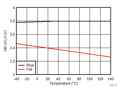
GUID-5B863553-CF5A-478F-9DC1-1E29132E473D-low.gif
Figure 6-15 HB UVLO Threshold
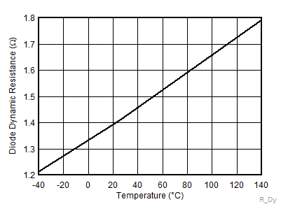
GUID-191C7C23-028F-48C9-9690-FFAB7647C11A-low.gif
Figure 6-17 Boot Diode Dynamic Resistance
GUID-50929761-498C-4133-9B56-0816B9B3733D-low.gif
IO=-100mA
Figure 6-19 LO High Output Voltage (VLOH)
GUID-FE771D21-DAEE-47F8-B9E6-66ADAF2F3770-low.gif
IO=-100mA
Figure 6-21 HO High Output Voltage (VHOH)
GUID-CF0AF6DC-9E13-41E7-A03A-901B1C214653-low.gif
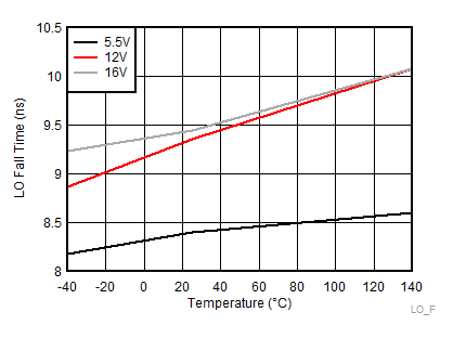
CL=1800pF
Figure 6-23 LO Fall Time
GUID-9A1B4E84-05C3-4A54-B737-CD7AF17EC4EC-low.gif
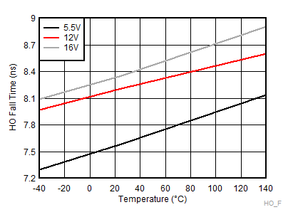
CL=1800pF
Figure 6-25 HO Fall Time
GUID-BAF545D4-2D8F-470B-AC95-C877D264A1BC-low.gif
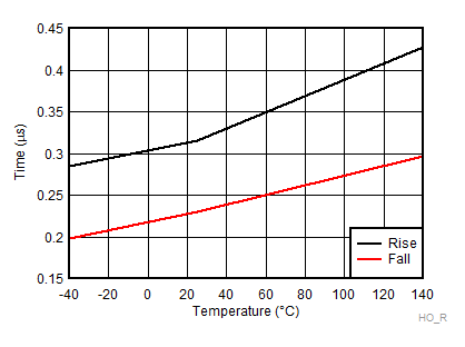
CL=100nF
Figure 6-27 HO Rise & Fall Time
GUID-8463EDC1-A276-4818-8123-DCADC436C5DF-low.gif
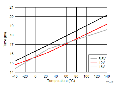
CL= No Load
Figure 6-29 HO Falling Propagation Delay (TDHFF)
GUID-28648DDC-CD46-4D3F-980A-72911B3ED7AF-low.gif
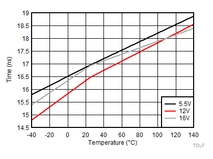
CL= No Load
Figure 6-31 LO Falling Propagation Delay (TDLFF)
GUID-82551056-0D00-440E-9C6A-1817056369A5-low.gif
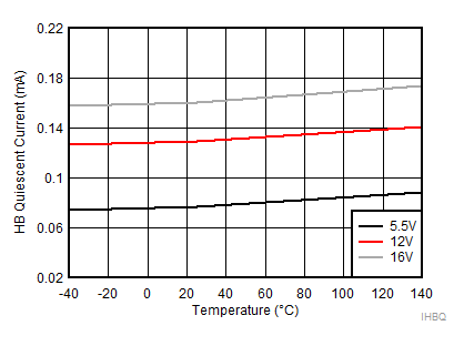
VHI = VLI = 0 V
Figure 6-2 HB Quiescent Current
GUID-AB3AB2BC-A4C9-45E3-AB71-841D6F4361EF-low.gif
CL = 0 FVDD =VHB= 12V
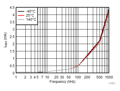
Figure 6-4 HB Operating Current
GUID-C913D565-3FAE-433F-B3E0-329B2FB13BED-low.gif
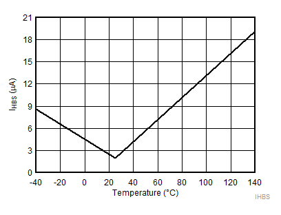
VHB=VHS=100V
Figure 6-6 HB to VSS Quiescent Current
GUID-94E98D21-7984-49C0-B4E3-8188121510E7-low.gif
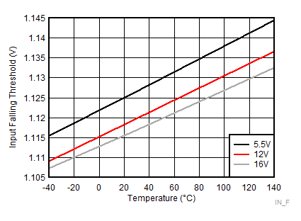
Figure 6-8 Input Falling Threshold
GUID-5AC96846-EAA1-4F2D-A8E6-8618687068DF-low.gif
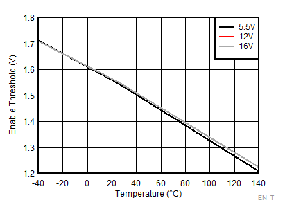
Figure 6-10 Enable Threshold
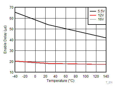
GUID-12C41414-D2CF-418B-A81A-EA1A410D5502-low.gif
Figure 6-12 Enable Delay
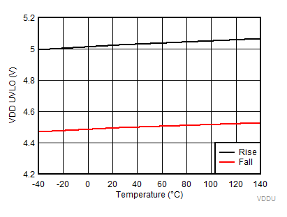
GUID-F55777A9-F819-4321-9C15-BCBF6185E5CA-low.gif
Figure 6-14 VDD UVLO Threshold
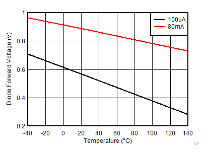
GUID-309053BA-3100-47D7-8DD2-2203AE77CECF-low.gif
Figure 6-16 Boot Diode Forward Voltage Drop
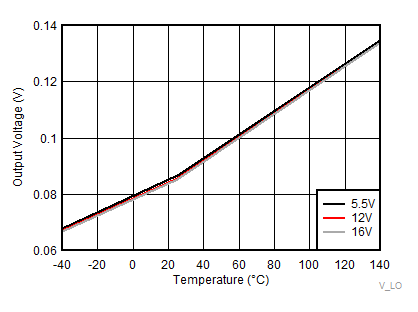
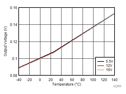
GUID-B819341A-A29D-4A0D-BE17-0B095147FC9F-low.gif
IO=100mA
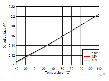
Figure 6-18 LO Low Output Voltage (VLOL)
GUID-F3F62501-9770-409C-B633-2570E8F2A7F7-low.gif
IO=100mA
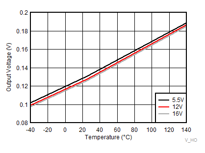
Figure 6-20 HO Low Output Voltage (VHOL)
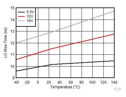
GUID-2BB3FABB-527B-49D8-B8A5-925E969C2690-low.gif
CL=1800pF
Figure 6-22 LO Rise Time
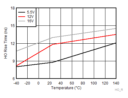
GUID-B0D9C656-DBBE-4EAF-8754-23C21A985506-low.gif
CL=1800pF
Figure 6-24 HO Rise Time
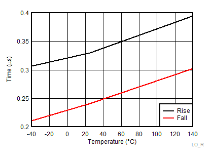
GUID-CC81EE82-77BF-4B45-8BE9-EA153AE7C68A-low.gif
CL=100nF
Figure 6-26 LO Rise & Fall Time
GUID-080201C1-F3A0-4D8E-9980-25A35CC451CC-low.gif
CL=No Load
Figure 6-28 HO Rising Propagation Delay (TDHRR)
GUID-50C81341-D5CC-4467-A76C-9CB72BD8976C-low.gif
CL= No Load
Figure 6-30 LO Rising Propagation Delay (TDLRR)