SLUSDU4A December 2020 – May 2022 UCC27289
PRODUCTION DATA
- 1 Features
- 2 Applications
- 3 Description
- 4 Revision History
- 5 Pin Configuration and Functions
- 6 Specifications
- 7 Detailed Description
- 8 Application and Implementation
- 9 Power Supply Recommendations
- 10Layout
- 11Device and Documentation Support
- 12Mechanical, Packaging, and Orderable Information
Package Options
Mechanical Data (Package|Pins)
Thermal pad, mechanical data (Package|Pins)
- DRC|10
Orderable Information
8.2.3 Application Curves
To minimize the switching losses in power supplies, turn-ON and turn-OFF of the power MOSFETs need to be as fast as possible. Higher the drive current capability of the driver, faster the switching. Therefore, the UCC27289 is designed with high drive current capability and low resistance of the output stages. One of the common way to test the drive capability of the gate driver device , is to test it under heavy load. Rise time and fall time of the outputs would provide idea of drive capability of the gate driver device. There should not be any resistance in series with the load capacitor if large capacitor is used to measure the drive strength. Peak current capability can be estimated using the fastest dV/dt along the rise and fall curve of the plot. This method is also useful in comparing performance of two or more gate driver devices.
UCC27289 was tested in application like environment. Synchrounous buck converter at no load was used to gnerate following waveforms. Switching frequency was set to 100kHz and input voltage was set to 100V. UCC27289 was driving BSC16DN250NS3 with 2 Ohm external resistor. All the waveforms were taken using single ended probes. Figure 8-3 and Figure 8-4 shows rise time and fall time of HO respectively. Figure 8-5 and Figure 8-6 shows rise time and fall time of LO respectively. Internal bootstrap diode and external bootstrap capacitor generated the high-side bias.
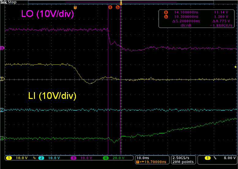
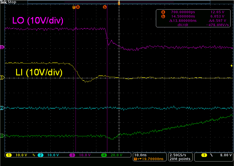
As explained in Section 8.2.2.5, propagation delay plays an important role in reliable operation of many applications. Figure 8-7 and Figure 8-8 shows LO rise and fall propagation delay of UCC27289. Similar propagation delay was observed for HO output as well.
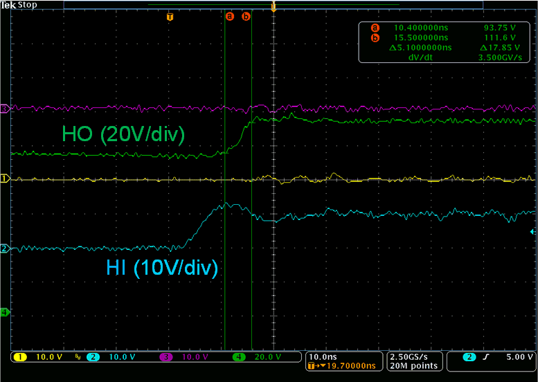
| VDD=12 V, HS=100V |
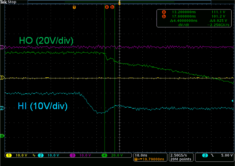
| VDD=12V, HS=100V |
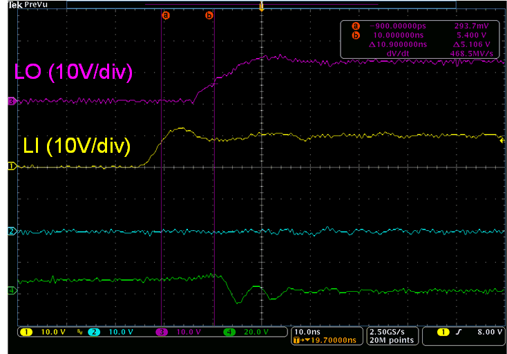
| VDD=12 V |
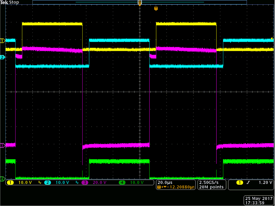
| VDD=10V, Vin=100V | CL=1nF | Ch1=HI Ch2=LI Ch3=HO Ch4=LO |

| VDD==12 V, HS=100V |
| VDD=12V, HS=100V |
| VDD=12 V |