SLUSEX3C April 2023 – July 2024 UCC27301A-Q1
PRODMIX
- 1
- 1 Features
- 2 Applications
- 3 Description
- 4 Pin Configuration and Functions
- 5 Specifications
- 6 Detailed Description
- 7 Application and Implementation
- 8 Power Supply Recommendations
- 9 Layout
- 10Device and Documentation Support
- 11Revision History
- 12Mechanical, Packaging, and Orderable Information
Package Options
Refer to the PDF data sheet for device specific package drawings
Mechanical Data (Package|Pins)
- DRC|10
- DDA|8
Thermal pad, mechanical data (Package|Pins)
Orderable Information
12.1 Tape and Reel Information
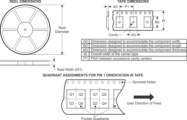
| Device | Package Type |
Package Drawing | Pins | SPQ | Reel Diameter (mm) |
Reel Width W1 (mm) |
A0 (mm) |
B0 (mm) |
K0 (mm) |
P1 (mm) |
W (mm) |
Pin1 Quadrant |
|---|---|---|---|---|---|---|---|---|---|---|---|---|
| PUCC27301AQDDARQ1 | SO | DDA | 8 | 3000 | 330.0 | 12.5 | 6.4 | 5.2 | 2.1 | 8.0 | 12.0 | Q1 |
| PUCC27301AQDRCRQ1 | VSON | DRC | 10 | 3000 | 330.0 | 12.4 | 3.3 | 3.3 | 1.1 | 8.0 | 12.0 | Q2 |
| UCC27301AQDDARQ1 | SO | DDA | 8 | 3000 | 330.0 | 12.5 | 6.4 | 5.2 | 2.1 | 8.0 | 12.0 | Q1 |
| UCC27301AQDRCRQ1 | VSON | DRC | 10 | 3000 | 330.0 | 12.4 | 3.3 | 3.3 | 1.1 | 8.0 | 12.0 | Q2 |
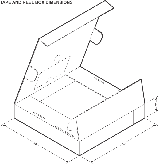
| Device | Package Type | Package Drawing | Pins | SPQ | Length (mm) | Width (mm) | Height (mm) |
|---|---|---|---|---|---|---|---|
| PUCC27301AQDDARQ1 | SO | DDA | 8 | 3000 | 340.5 | 336.1 | 25 |
| PUCC27301AQDRCRQ1 | VSON | DRC | 10 | 3000 | 367.0 | 367.0 | 35 |
| UCC27301AQDDARQ1 | SO | DDA | 8 | 3000 | 340.5 | 336.1 | 25 |
| UCC27301AQDRCRQ1 | VSON | DRC | 10 | 3000 | 367.0 | 367.0 | 35 |