SLUSA13E February 2010 – November 2023 UCC27321-Q1 , UCC27322-Q1
PRODUCTION DATA
- 1
- 1 Features
- 2 Applications
- 3 Description
- 4 Description (continued)
- 5 Related Products
- 6 Pin Configuration and Functions
- 7 Specifications
- 8 Detailed Description
- 9 Application and Implementation
- 10Power Supply Recommendations
- 11Layout
- 12Device and Documentation Support
- 13Revision History
- 14Mechanical, Packaging, and Orderable Information
Package Options
Mechanical Data (Package|Pins)
Thermal pad, mechanical data (Package|Pins)
- DGN|8
Orderable Information
7.7 Typical Characteristics
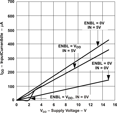 Figure 7-3 Input Current Idle vs Supply Voltage (UCC27321-Q1)
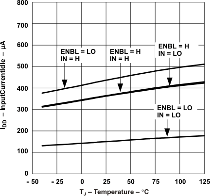 Figure 7-5 Input Current Idle vs Temperature (UCC27321-Q1)
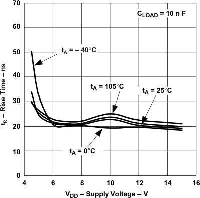 Figure 7-7 Rise Time vs Supply Voltage
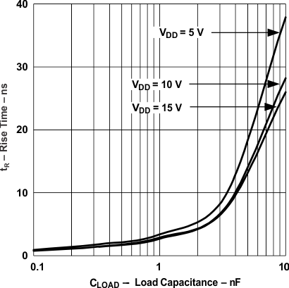 Figure 7-9 Rise Time vs Load Capacitance
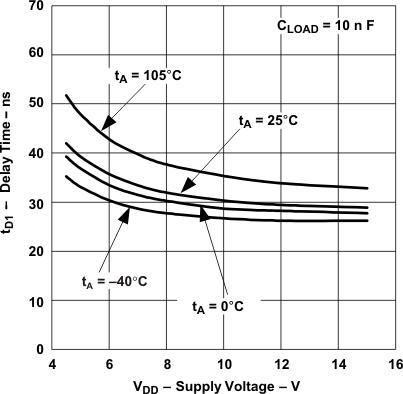 Figure 7-11 tD1 Delay Time vs Supply Voltage
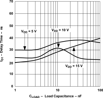 Figure 7-13 tD1 Delay Time vs Load Capacitance
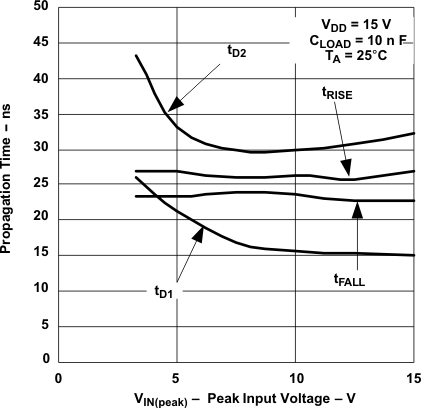 Figure 7-15 Propagation Times vs Peak Input Voltage
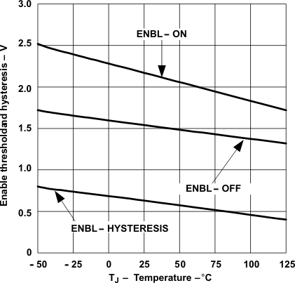 Figure 7-17 Enable Threshold and Hysteresis vs Temperature
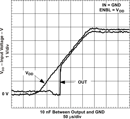 Figure 7-19 Output Behavior vs VDD (UCC27321-Q1)
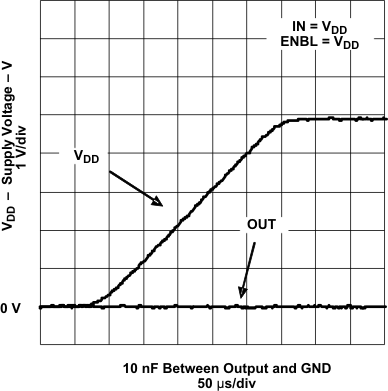 Figure 7-21 Output Behavior vs VDD (Inverting)
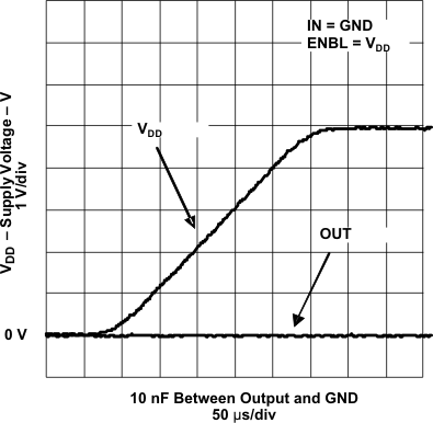 Figure 7-23 Output Behavior vs VDD (Noninverting)
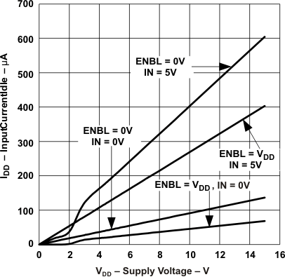 Figure 7-4 Input Current Idle vs Supply Voltage (UCC27322-Q1)
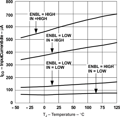 Figure 7-6 Input Current Idle vs Temperature (UCC27322-Q1)
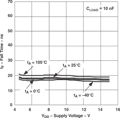 Figure 7-8 Fall Time vs Supply Voltage
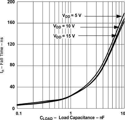 Figure 7-10 Fall Time vs Output Capacitance
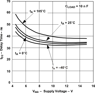 Figure 7-12 tD2 Delay Time vs Supply Voltage
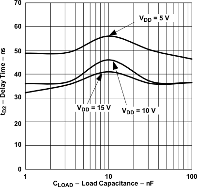 Figure 7-14 tD2 Delay Time vs Load Capacitance
 Figure 7-16 Input
Threshold vs Supply Voltage
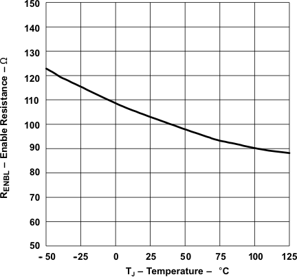 Figure 7-18 Enable Resistance vs Temperature
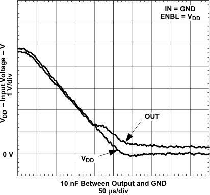 Figure 7-20 Output Behavior vs VDD (UCC27321-Q1)
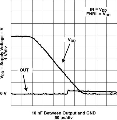 Figure 7-22 Output Behavior vs VDD (Inverting)
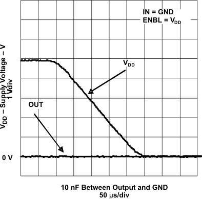 Figure 7-24 Output Behavior vs VDD (Noninverting)