SLUS678D March 2008 – November 2023 UCC27324-Q1
PRODUCTION DATA
- 1
- 1 Features
- 2 Applications
- 3 Description
- 4 Pin Configuration and Functions
-
5 Specifications
- 5.1 Absolute Maximum Ratings
- 5.2 ESD Ratings
- 5.3 Recommended Operating Conditions
- 5.4 Thermal Information
- 5.5 Overall Electrical Characteristics
- 5.6 Power Dissipation Characteristics
- 5.7 Input (INA, INB) Electrical Characteristics
- 5.8 Output (OUTA, OUTB) Electrical Characteristics
- 5.9 Switching Characteristics
- 5.10 Typical Characteristics
- 6 Detailed Description
- 7 Application and Implementation
- 8 Power Supply Recommendations
- 9 Layout
- 10Device and Documentation Support
- 11Revision History
- 12Mechanical, Packaging, and Orderable Information
Package Options
Mechanical Data (Package|Pins)
- D|8
Thermal pad, mechanical data (Package|Pins)
Orderable Information
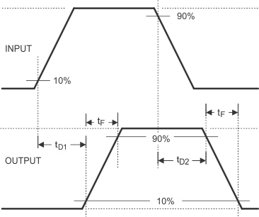
5.9 Switching Characteristics
VCC = 4.5 V to 15 V, TA = –40°C to 125°C (unless otherwise noted) (see
Figure 5-1)
| PARAMETER | TEST CONDITIONS | MIN | TYP | MAX | UNIT | |
|---|---|---|---|---|---|---|
| tR | Rise time (OUTA, OUTB) | CLOAD = 1.8 nF | 20 | 40 | ns | |
| tF | Fall time (OUTA, OUTB) | CLOAD = 1.8 nF | 15 | 40 | ns | |
| tD1 | Delay time, IN rising (IN to OUT) | CLOAD = 1.8 nF | 25 | 40 | ns | |
| tD2 | Delay time, IN falling (IN to OUT) | CLOAD = 1.8 nF | 35 | 50 | ns | |
 Figure 5-1 Switching
Waveforms for Noninverting Driver