SLUS678D March 2008 – November 2023 UCC27324-Q1
PRODUCTION DATA
- 1
- 1 Features
- 2 Applications
- 3 Description
- 4 Pin Configuration and Functions
-
5 Specifications
- 5.1 Absolute Maximum Ratings
- 5.2 ESD Ratings
- 5.3 Recommended Operating Conditions
- 5.4 Thermal Information
- 5.5 Overall Electrical Characteristics
- 5.6 Power Dissipation Characteristics
- 5.7 Input (INA, INB) Electrical Characteristics
- 5.8 Output (OUTA, OUTB) Electrical Characteristics
- 5.9 Switching Characteristics
- 5.10 Typical Characteristics
- 6 Detailed Description
- 7 Application and Implementation
- 8 Power Supply Recommendations
- 9 Layout
- 10Device and Documentation Support
- 11Revision History
- 12Mechanical, Packaging, and Orderable Information
Package Options
Mechanical Data (Package|Pins)
- D|8
Thermal pad, mechanical data (Package|Pins)
Orderable Information
3 Description
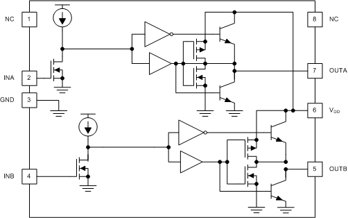
The UCC27324-Q1 high-speed dual-MOSFET driver can deliver large peak currents into capacitive loads. Using a design that inherently minimizes shoot-through current, these drivers deliver 4 A of current where it is needed most, at the Miller plateau region during the MOSFET switching transition. A unique bipolar and MOSFET hybrid output stage in parallel also allows efficient current sourcing and sinking at low supply voltages.
The device is offered in a standard SOIC-8 (D) package.
Device
Information
| PART NUMBER | PACKAGE(1) | BODY SIZE (NOM) |
|---|---|---|
| UCC27324-Q1 | SOIC (8) | 4.90 mm × 3.91 mm |
(1) For all available packages, see the orderable addendum at the end of the datasheet.
 Block Diagram