SLUSB33A May 2012 – December 2014 UCC27518 , UCC27519
PRODUCTION DATA.
- 1 Features
- 2 Applications
- 3 Description
- 4 Revision History
- 5 Description (continued)
- 6 Device Comparison Table
- 7 Pin Configuration and Functions
- 8 Specifications
- 9 Detailed Description
- 10Application and Implementation
- 11Power Supply Recommendations
- 12Layout
- 13Device and Documentation Support
- 14Mechanical, Packaging, and Orderable Information
Package Options
Mechanical Data (Package|Pins)
- DBV|5
Thermal pad, mechanical data (Package|Pins)
Orderable Information
1 Features
- Low-Cost, Gate-Driver Device Offering Superior Replacement of NPN and PNP Discrete Solutions
- Pin-to-Pin Compatible With TI's TPS2828 and TPS2829 devices
- 4-A Peak Source and 4-A Peak Sink Symmetrical Drive
- Fast Propagation Delays (17-ns Typical)
- Fast Rise and Fall Times (8-ns and 7-ns Typical)
- 4.5-V to 18-V Single Supply Range
- Outputs Held Low During VDD UVLO (Ensures Glitch-Free Operation at Power Up and Power Down)
- CMOS Input Logic Threshold (Function of Supply Voltage With Hysteresis)
- Hysteretic Logic Thresholds for High Noise Immunity
- EN Pin for Enable Function (Allowed to Be No Connect)
- Output Held Low when Input Pins are Floating
- Input Pin Absolute Maximum Voltage Levels Not Restricted by VDD Pin Bias Supply Voltage
- Operating Temperature Range of –40°C to 140°C
- 5-Pin DBV Package (SOT-23)
2 Applications
- Switched-Mode Power Supplies
- DC-DC Converters
- Companion Gate Driver Devices for Digital Power Controllers
- Solar Power, Motor Control, UPS
- Gate Driver for Emerging Wide Band-Gap Power Devices (Such as GaN)
3 Description
The UCC27518 and UCC27519 single-channel, high-speed, low-side gate driver device can effectively drive MOSFET and IGBT power switches. Using a design that inherently minimizes shoot-through current, UCC27518 and UCC27519 can source and sink high, peak-current pulses into capacitive loads offering rail-to-rail drive capability and extremely small propagation delay typically 17 ns.
The UCC27518 and UCC27519 provide 4-A source, 4-A sink (symmetrical drive) peak-drive current capability at VDD = 12 V.
The UCC27518 and UCC27519 are designed to operate over a wide VDD range of 4.5 V to 18 V and a wide temperature range of –40°C to 140°C. Internal under voltage lockout (UVLO) circuitry on the VDD pin holds output low outside VDD operating range. The capability to operate at low voltage levels such as below 5 V, along with best-in-class switching characteristics, is especially suited for driving emerging wide band-gap power switching devices such as GaN power semiconductor devices.
Device Information(1)
| PART NUMBER | PACKAGE | BODY SIZE (NOM) |
|---|---|---|
| UCC27518 | SOT-23 (5) | 2.90 mm × 1.60 mm |
| UCC27519 |
- For all available packages, see the orderable addendum at the end of the datasheet.
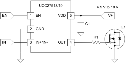
Typical Application Diagram
