SLVSC90B August 2013 – August 2015 UCC27518A-Q1 , UCC27519A-Q1
PRODUCTION DATA.
- 1 Features
- 2 Applications
- 3 Description
- 4 Revision History
- 5 Description (continued)
- 6 Device Comparison Table
- 7 Pin Configuration and Functions
- 8 Specifications
- 9 Detailed Description
- 10 Application and Implementation
- 11Power Supply Recommendations
- 12Layout
- 13Device and Documentation Support
- 14Mechanical, Packaging, and Orderable Information
Package Options
Refer to the PDF data sheet for device specific package drawings
Mechanical Data (Package|Pins)
- DBV|5
Thermal pad, mechanical data (Package|Pins)
Orderable Information
7 Pin Configuration and Functions
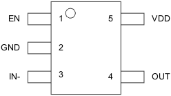
UCC27518A-Q1 DBV Package
5-Pin SOT-23
Top View

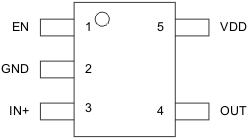
UCC27519A-Q1 DBV Package
5-Pin SOT-23
Top View

Pin Functions
| PIN | I/O | DESCRIPTION | |
|---|---|---|---|
| NO. | NAME | ||
| 1 | EN | I | Enable input. When the EN pin is biased LOW, the output is disabled regardless of input state. When the EN pin is biased high or left floating, the output is enabled. The EN pin is allowed to float because it is pin-to-pin compatible with the NC pin of the TPS282x device. |
| 2 | GND | — | Ground. All signals are referenced to this pin. |
| 3 | IN– (UCC27518A-Q1) | I | Input. This pin is the inverting input in the UCC27518A-Q1 device. The output is held LOW if the IN– pin is unbiased or floating. |
| IN+ (UCC27519A-Q1) | I | Input. This pin is the noninverting input in the UCC27519A-Q1 device. The output is held LOW if the IN+ pin is unbiased or floating. | |
| 4 | OUT | O | Sourcing and sinking current output of driver. |
| 5 | VDD | I | Supply input. |