SLUSBP4C August 2013 – June 2024 UCC27524A
PRODUCTION DATA
- 1
- 1 Features
- 2 Applications
- 3 Description
- 4 Pin Configuration and Functions
- 5 Specifications
- 6 Detailed Description
- 7 Application and Implementation
- 8 Power Supply Recommendations
- 9 Layout
- 10Device and Documentation Support
- 11Revision History
- 12Mechanical, Packaging, and Orderable Information
Package Options
Mechanical Data (Package|Pins)
Thermal pad, mechanical data (Package|Pins)
- DGN|8
Orderable Information
3 Description
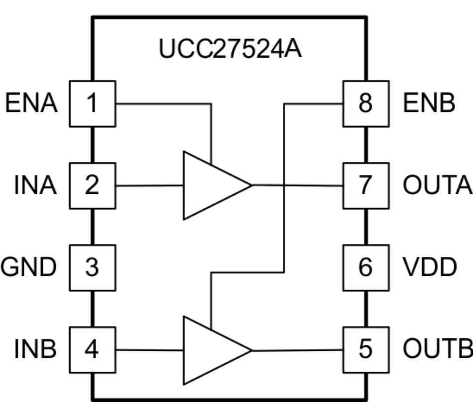
The UCC27524A device is a dual-channel, high-speed, low-side, gate-driver device capable of effectively driving MOSFET and IGBT power switches. The UCC27524A is a variant of the UCC2752x family. The UCC27524A adds the ability to handle –5V directly at the input pins for increased robustness. The UCC27524A is a dual non-inverting driver. Using a design that inherently minimizes shoot-through current, the UCC27524A is capable of delivering high-peak current pulses of up to 5A source and 5A sink into capacitive loads along with rail-to-rail drive capability and extremely small propagation delay typically 17ns. In addition, the drivers feature matched internal propagation delays between the two channels which are very well suited for applications requiring dual-gate drives with critical timing, such as synchronous rectifiers. This also enables connecting two channels in parallel to effectively increase current-drive capability or driving two switches in parallel with a single input signal. The input pin thresholds are based on TTL and CMOS compatible low-voltage logic, which is fixed and independent of the VDD supply voltage. Wide hysteresis between the high and low thresholds offers excellent noise immunity.
| PART NUMBER | PACKAGE(1) | BODY SIZE (NOM) |
|---|---|---|
| UCC27524A | D (SOIC 8) | 4.90mm x 3.91mm |
| DGN (HVSSOP 8) | 3.00mm x 3.00mm |
 Dual Non-Inverting Inputs