SLUSBP4C August   2013  – June 2024 UCC27524A

PRODUCTION DATA  

  1.   1
  2. Features
  3. Applications
  4. Description
  5. Pin Configuration and Functions
  6. Specifications
    1. 5.1 Absolute Maximum Ratings
    2. 5.2 ESD Ratings
    3. 5.3 Recommended Operating Conditions
    4. 5.4 Thermal Information
    5. 5.5 Electrical Characteristics
    6. 5.6 Switching Characteristics
    7. 5.7 Timing Diagrams
    8. 5.8 Typical Characteristics
  7. Detailed Description
    1. 6.1 Overview
    2. 6.2 Functional Block Diagram
    3. 6.3 Feature Description
      1. 6.3.1 Operating Supply Current
      2. 6.3.2 Input Stage
      3. 6.3.3 Enable Function
      4. 6.3.4 Output Stage
    4. 6.4 Low Propagation Delays and Tightly Matched Outputs
    5. 6.5 Device Functional Modes
  8. Application and Implementation
    1. 7.1 Application Information
    2. 7.2 Typical Application
      1. 7.2.1 Design Requirements
      2. 7.2.2 Detailed Design Procedure
        1. 7.2.2.1 VDD and Undervoltage Lockout
        2. 7.2.2.2 Drive Current and Power Dissipation
      3. 7.2.3 Application Curves
  9. Power Supply Recommendations
  10. Layout
    1. 9.1 Layout Guidelines
    2. 9.2 Layout Example
    3. 9.3 Thermal Considerations
  11. 10Device and Documentation Support
    1. 10.1 Device Support
      1. 10.1.1 Third-Party Products Disclaimer
    2. 10.2 Receiving Notification of Documentation Updates
    3. 10.3 Support Resources
    4. 10.4 Trademarks
    5. 10.5 Electrostatic Discharge Caution
    6. 10.6 Glossary
  12. 11Revision History
  13. 12Mechanical, Packaging, and Orderable Information

Package Options

Mechanical Data (Package|Pins)
Thermal pad, mechanical data (Package|Pins)
Orderable Information

Typical Characteristics

Unless otherwise specified, VDD=12 V, INx = 3.3 V, ENx = 3.3 V, TJ = 25°C, no load
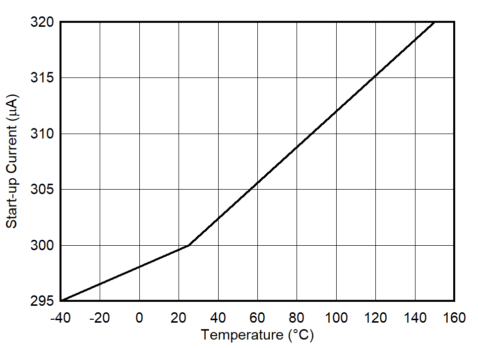
UCC27524A Start-Up and Quiescent
                        Current
Figure 5-3 Start-Up and Quiescent Current
UCC27524A Static Supply Current (Outputs in DC On or Off Condition)
Figure 5-5 Static Supply Current (Outputs in DC On or Off Condition)
UCC27524A VDD
                        UVLO Threshold
Figure 5-7 VDD UVLO Threshold
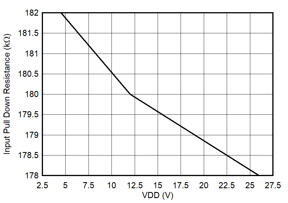
UCC27524A Input
                        Pulldown Resistance
Figure 5-9 Input Pulldown Resistance
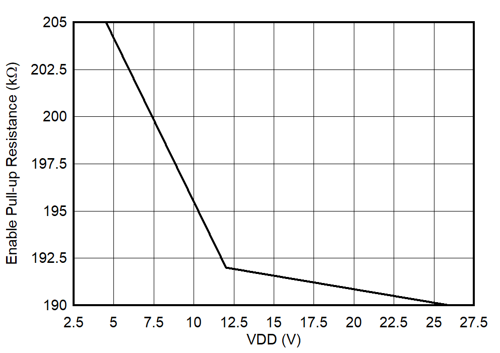
UCC27524A Enable Pullup Resistance
Figure 5-11 Enable Pullup Resistance
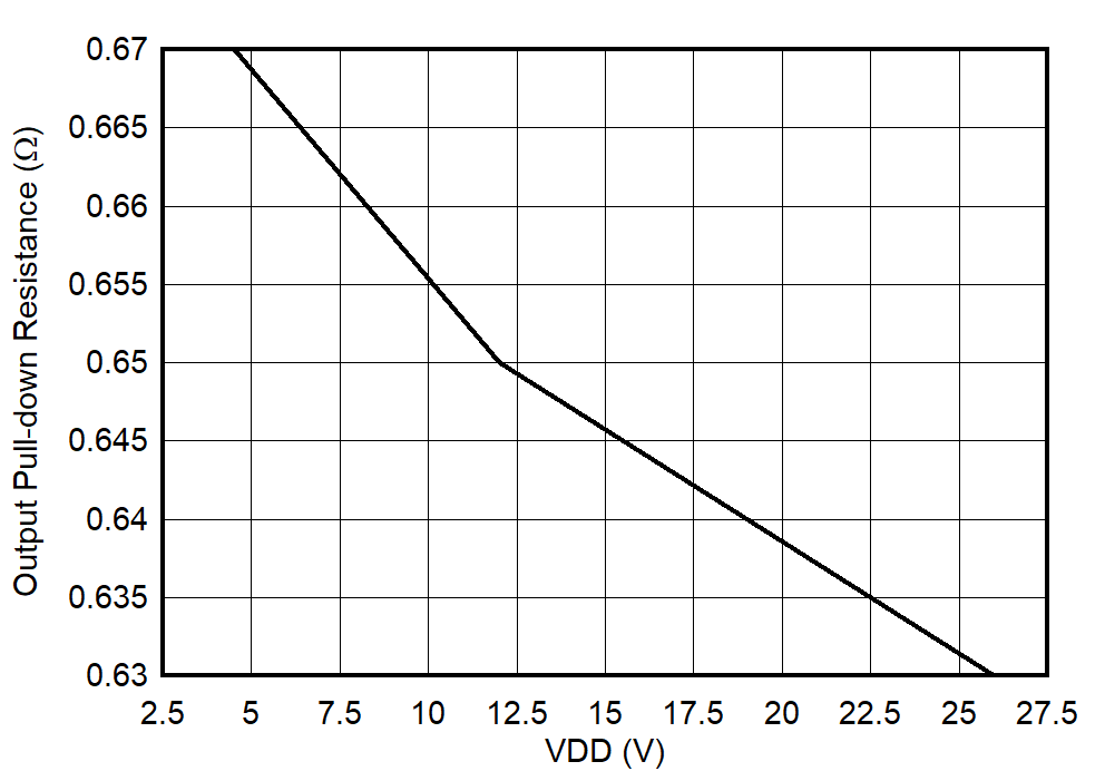
UCC27524A Output Pulldown Resistance
Figure 5-13 Output Pulldown Resistance
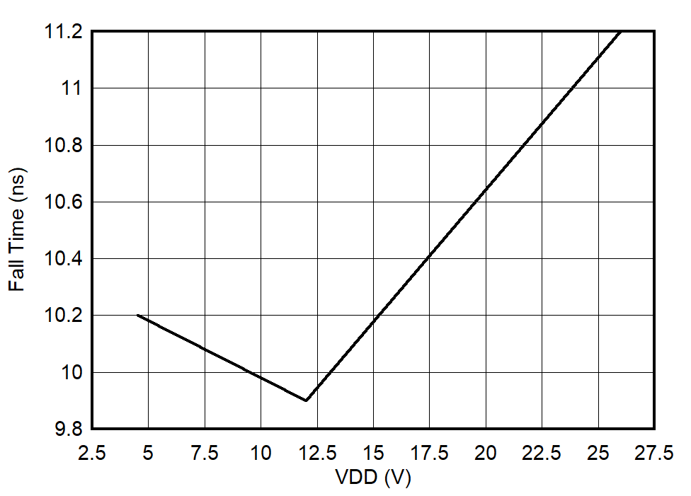
UCC27524A Output Fall Time vs VDD
CLOAD = 1.8 nF
Figure 5-15 Output Fall Time vs VDD
UCC27524A Input
                        to Output Rising (Turn-On) Propagation Delay vs VDD
CLOAD = 1.8 nF
Figure 5-17 Input to Output Rising (Turn-On) Propagation Delay vs VDD
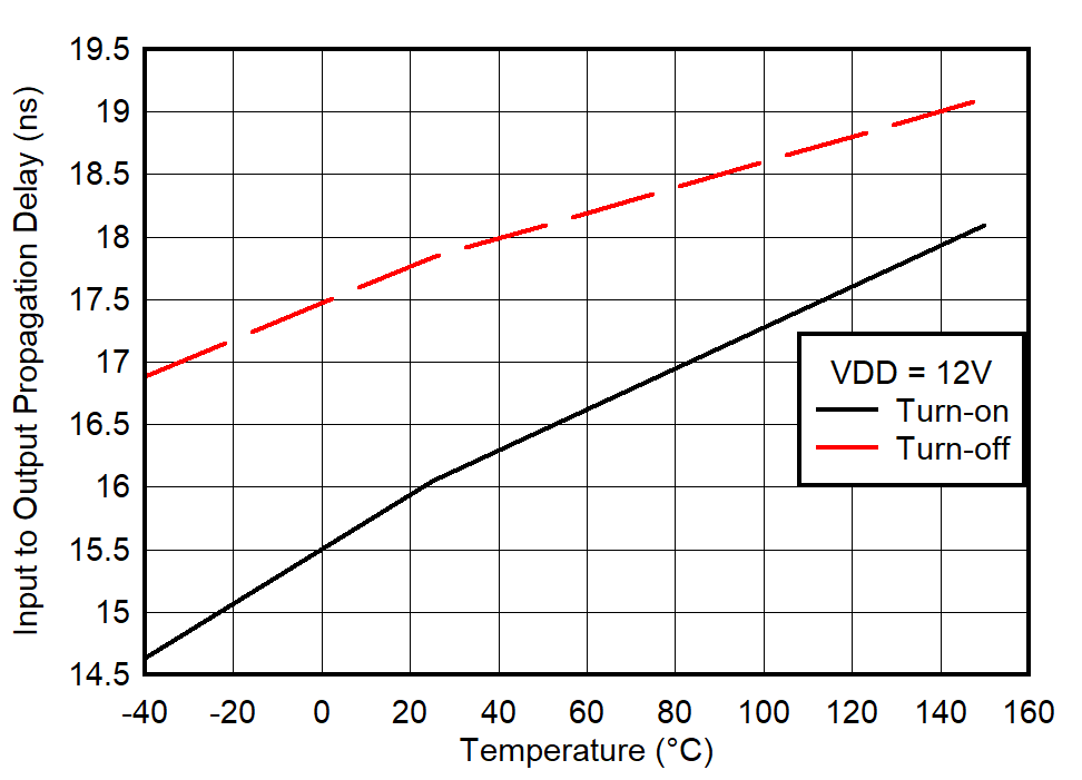
UCC27524A Input Propagation Delay vs
                        Temperature
CLOAD = 1.8 nF
Figure 5-19 Input Propagation Delay vs Temperature
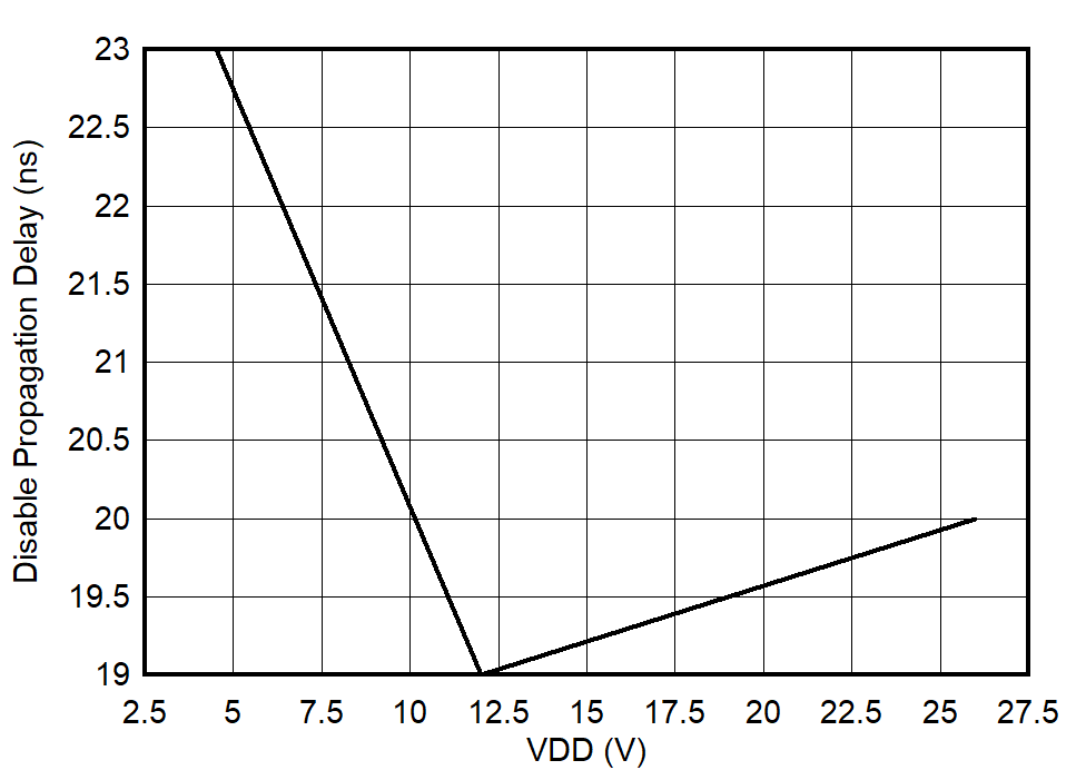
UCC27524A Enable to Output Falling Propagation Delay
CLOAD = 1.8 nF
Figure 5-21 Enable to Output Falling Propagation Delay
UCC27524A Turn-Off and Falling Delay Matching
Figure 5-23 Turn-Off and Falling Delay Matching
UCC27524A Peak
                        Sink Current vs VDD
Figure 5-25 Peak Sink Current vs VDD
UCC27524A Operating Supply Current (Both Outputs Switching)
Figure 5-4 Operating Supply Current (Both Outputs Switching)
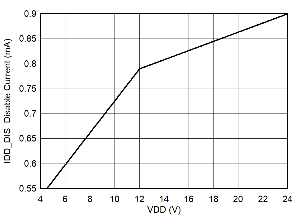
UCC27524A Disable Current (EN = 0 V)
Figure 5-6 Disable Current (EN = 0 V)
UCC27524A Input
                        Thresholds
Figure 5-8 Input Thresholds
UCC27524A Enable Threshold
Figure 5-10 Enable Threshold
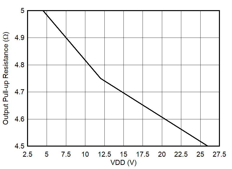
UCC27524A Output Pullup Resistance
Figure 5-12 Output Pullup Resistance
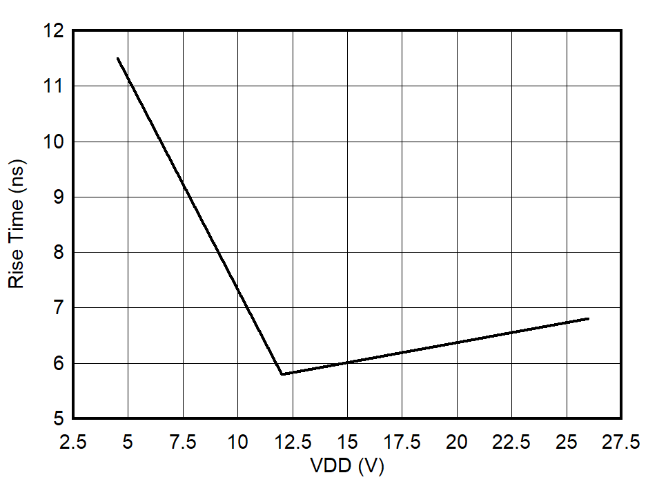
UCC27524A Output Rise Time vs VDD
CLOAD = 1.8 nF
Figure 5-14 Output Rise Time vs VDD
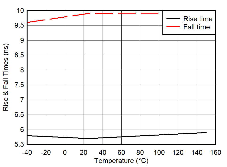
UCC27524A Output Rise and Fall Time vs
                        Temperature
CLOAD = 1.8 nF
Figure 5-16 Output Rise and Fall Time vs Temperature
UCC27524A Input
                        to Output Falling (Turn-Off) Propagation Delay vs VDD
CLOAD = 1.8 nF
Figure 5-18 Input to Output Falling (Turn-Off) Propagation Delay vs VDD
UCC27524A Enable to Output Rising Propagation Delay
CLOAD = 1.8 nF
Figure 5-20 Enable to Output Rising Propagation Delay
UCC27524A Turn-on/Rising Delay Matching
Figure 5-22 Turn-on/Rising Delay Matching
UCC27524A Peak
                        Source Current vs VDD
Figure 5-24 Peak Source Current vs VDD