SLVSDH6A April 2017 – June 2024 UCC27524A1-Q1
PRODUCTION DATA
- 1
- 1 Features
- 2 Applications
- 3 Description
- 4 Description (continued)
- 5 Pin Configuration and Functions
- 6 Specifications
- 7 Detailed Description
- 8 Application and Implementation
- 9 Power Supply Recommendations
- 10Layout
- 11Device and Documentation Support
- 12Revision History
- 13Mechanical, Packaging, and Orderable Information
Package Options
Mechanical Data (Package|Pins)
- DGN|8
Thermal pad, mechanical data (Package|Pins)
- DGN|8
Orderable Information
3 Description
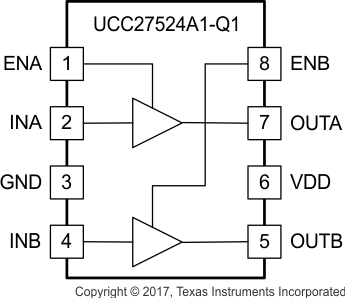
The UCC27524A1-Q1 device is a dual-channel, high-speed, low-side, gate-driver device capable of effectively driving MOSFET and IGBT power switches. The UCC27524A1-Q1 device is a variant of the UCC2752x family. The UCC27524A1-Q1 device adds the ability to handle –5V directly at the input pins for increased robustness. The UCC27524A1-Q1 device is a dual, non-inverting driver. Using a design that inherently minimizes shoot-through current, the UCC27524A1-Q1 device is capable of delivering high-peak current pulses of up to 5A source and 5A sink into capacitive loads along with rail-to-rail drive capability and extremely small propagation delay (typically 17ns). In addition, the drivers feature matched, internal-propagation delays between the two channels which are very well suited for applications requiring dual-gate drives with critical timing, such as synchronous rectifiers. This also enables connecting two channels in parallel to effectively increase current-drive capability or driving two switches in parallel with a single input signal. The input pin thresholds are based on TTL and CMOS compatible low-voltage logic, which is fixed and independent of the VDD supply voltage. Wide hysteresis between the high and low thresholds offers excellent noise immunity.
| PART NUMBER | PACKAGE(1) | BODY SIZE (NOM) |
|---|---|---|
| UCC27524A1-Q1 | DGN (MSOP-PowerPAD, 8) | 3.00mm × 3.00mm |
 Dual Noninverting Inputs