SLVSDH6A April 2017 – June 2024 UCC27524A1-Q1
PRODUCTION DATA
- 1
- 1 Features
- 2 Applications
- 3 Description
- 4 Description (continued)
- 5 Pin Configuration and Functions
- 6 Specifications
- 7 Detailed Description
- 8 Application and Implementation
- 9 Power Supply Recommendations
- 10Layout
- 11Device and Documentation Support
- 12Revision History
- 13Mechanical, Packaging, and Orderable Information
Package Options
Mechanical Data (Package|Pins)
- DGN|8
Thermal pad, mechanical data (Package|Pins)
- DGN|8
Orderable Information
8.2.2.1 VDD and Undervoltage Lockout
The UCC27524A1-Q1 device has an internal undervoltagelockout (UVLO) protection feature on the VDD pin supply circuit blocks. When VDD is rising and the level is still below UVLO threshold, this circuit holds the output low, regardless of the status of the inputs. The UVLO is typically 4 V with 300-mV typical hysteresis. This hysteresis prevents chatter when low VDD supply voltages have noise from the power supply and also when there are droops in the VDD bias voltage when the system commences switching and there is a sudden increase in IDD. The capability to operate at low voltage levels such as below 5 V, along with best in class switching characteristics, is especially suited for driving emerging GaN power semiconductor devices.
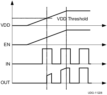
For example, at power up, the UCC27524A1-Q1 driver-device output remains low until the VDD voltage reaches the UVLO threshold if enable pin is active or floating. The magnitude of the OUT signal rises with VDD until steady-state VDD is reached. The operation in Figure 8-2 shows that the output remains low until the UVLO threshold is reached, and then the output is in-phase with the input.
Because the device draws current from the VDD pin to bias all internal circuits, for the best high-speed circuit performance, two VDD bypass capacitors are recommended to prevent noise problems. The use of surface mount components is highly recommended. A 0.1-μF ceramic capacitor must be located as close as possible to the VDD to GND pins of the gate-driver device. In addition, a larger capacitor (such as 1-μF) with relatively low ESR must be connected in parallel and close proximity to help deliver the high-current peaks required by the load. The parallel combination of capacitors presents a low impedance characteristic for the expected current levels and switching frequencies in the application.
 Figure 8-2 Power-Up
Noninverting Driver