SLUSAQ3H November 2011 – June 2024 UCC27523 , UCC27525 , UCC27526
PRODUCTION DATA
- 1
- 1 Features
- 2 Applications
- 3 Description
- 4 Description (continued)
- 5 Pin Configuration and Functions
- 6 Specifications
- 7 Detailed Description
- 8 Application and Implementation
- 9 Power Supply Recommendations
- 10Layout
- 11Device and Documentation Support
- 12Revision History
- 13Mechanical, Packaging, and Orderable Information
Package Options
Mechanical Data (Package|Pins)
- DSD|8
Thermal pad, mechanical data (Package|Pins)
- DSD|8
Orderable Information
8.2.2.5 Drive Current and Power Dissipation
The UCC27523/5/6 family of drivers are capable of delivering 5-A of current to a MOSFET gate for a period of several-hundred nanoseconds at VDD = 12 V. High peak current is required to turn the device ON quickly. Then, to turn the device OFF, the driver is required to sink a similar amount of current to ground which repeats at the operating frequency of the power device. The power dissipated in the gate-driver device package depends on the following factors:
- Gate charge required of the power MOSFET (usually a function of the drive voltage VGS, which is very close to input bias supply voltage VDD due to low VOH drop-out)
- Switching frequency
- Use of external gate resistors
Because UCC2752x features very low quiescent currents and internal logic to eliminate any shoot-through in the output driver stage, their effect on the power dissipation within the gate driver can be safely assumed to be negligible.
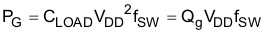
When a driver device is tested with a discrete, capacitive load calculating the power that is required from the bias supply is fairly simple. The energy that must be transferred from the bias supply to charge the capacitor is given by Equation 1.
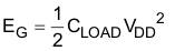
where
- CLOAD is load capacitor
- VDD is bias voltage feeding the driver.
There is an equal amount of energy dissipated when the capacitor is charged. This leads to a total power loss given by Equation 2.
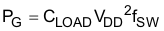
where
- fSW is the switching frequency
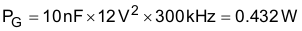
With VDD = 12 V, CLOAD = 10 nF and ƒSW = 300 kHz the power loss is calculated as (see Equation 3):
The switching load presented by a power MOSFET is converted to an equivalent capacitance by examining the gate charge required to switch the device. This gate charge includes the effects of the input capacitance plus the added charge needed to swing the drain voltage of the power device as it switches between the ON and OFF states. Most manufacturers provide specifications that provide the typical and maximum gate charge, in nC, to switch the device under specified conditions. Using the gate charge Qg, the power that must be dissipated when charging a capacitor is determined which by using the equivalence Qg = CLOADVDD to provide Equation 4 for power:
Assuming that UCC2752x is driving power MOSFET with 60 nC of gate charge (Qg = 60 nC at VDD = 12 V) on each output, the gate charge related power loss is calculated as (see Equation 5):

This power PG is dissipated in the resistive elements of the circuit when the MOSFET turns on or turns off. Half of the total power is dissipated when the load capacitor is charged during turnon, and the other half is dissipated when the load capacitor is discharged during turnoff. When no external gate resistor is employed between the driver and MOSFET/IGBT, this power is completely dissipated inside the driver package. With the use of external gate drive resistors, the power dissipation is shared between the internal resistance of driver and external gate resistor in accordance to the ratio of the resistances (more power dissipated in the higher resistance component). Based on this simplified analysis, the driver power dissipation during switching is calculated as follows (see Equation 6):
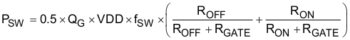
where
- ROFF = ROL
- RON (effective resistance of pullup structure) = 1.5 x ROL
In addition to the above gate-charge related power dissipation, additional dissipation in the driver is related to the power associated with the quiescent bias current consumed by the device to bias all internal circuits such as input stage (with pullup and pulldown resistors), enable, and UVLO sections. As shown in Figure 6-6, the quiescent current is less than 0.6 mA even in the highest case. The quiescent power dissipation is calculated easily with Equation 7.
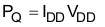
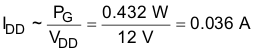
Assuming , IDD = 6 mA, the power loss is:
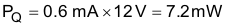
Clearly, this power loss is insignificant compared to gate charge related power dissipation calculated earlier.
With a 12-V supply, the bias current is estimated as follows, with an additional 0.6-mA overhead for the quiescent consumption: