SLVSCE4C December   2013  – September 2024 UCC27532-Q1

PRODUCTION DATA  

  1.   1
  2. Features
  3. Applications
  4. Description
  5. Description (continued)
  6. Pin Configuration and Functions
  7. Specifications
    1. 6.1 Absolute Maximum Ratings
    2. 6.2 ESD Ratings
    3. 6.3 Recommended Operating Conditions
    4. 6.4 Thermal Information
    5. 6.5 Electrical Characteristics
    6. 6.6 Switching Characteristics
    7. 6.7 Typical Characteristics
  8. Detailed Description
    1. 7.1 Overview
    2. 7.2 Functional Block Diagram
    3. 7.3 Feature Description
      1. 7.3.1 VDD Undervoltage Lockout
      2. 7.3.2 Input Stage
      3. 7.3.3 Enable Function
      4. 7.3.4 Output Stage
    4. 7.4 Device Functional Modes
  9. Application and Implementation
    1. 8.1 Application Information
    2. 8.2 Typical Applications
      1. 8.2.1 Driving IGBT Without Negative Bias
        1. 8.2.1.1 Design Requirements
        2. 8.2.1.2 Detailed Design Procedure
          1. 8.2.1.2.1 Input-to-Output Configuration
          2. 8.2.1.2.2 Input Threshold Type
          3. 8.2.1.2.3 VDD Bias Supply Voltage
          4. 8.2.1.2.4 Peak Source and Sink Currents
          5. 8.2.1.2.5 Enable and Disable Function
          6. 8.2.1.2.6 Propagation Delay
          7. 8.2.1.2.7 Power Dissipation
        3. 8.2.1.3 Application Curves
      2. 8.2.2 Driving IGBT With 13-V Negative Turnoff Bias
      3. 8.2.3 Using UCC27532-Q1 Drivers in an Inverter
  10. Power Supply Recommendations
  11. 10Layout
    1. 10.1 Layout Guidelines
    2. 10.2 Layout Example
    3. 10.3 Thermal Consideration
  12. 11Device and Documentation Support
    1. 11.1 Third-Party Products Disclaimer
    2. 11.2 Documentation Support
      1. 11.2.1 Related Documentation
    3. 11.3 Receiving Notification of Documentation Updates
    4. 11.4 Support Resources
    5. 11.5 Trademarks
    6. 11.6 Electrostatic Discharge Caution
    7. 11.7 Glossary
  13. 12Revision History
  14. 13Mechanical, Packaging, and Orderable Information

Package Options

Mechanical Data (Package|Pins)
Thermal pad, mechanical data (Package|Pins)
Orderable Information

Pin Configuration and Functions

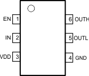
UCC27532-Q1 DBV Package6-Pin SOT-23
                    Top View Figure 5-1 DBV Package6-Pin SOT-23 Top View
Table 5-1 Pin Functions
PIN I/O DESCRIPTION
NAME NO.
EN 1 I Enable
(Pull EN to GND to disable output, pull it high or leave it open to enable the output)
GND 4 Ground (all signals are referenced to this node)
IN 2 I Driver noninverting input (CMOS threshold)
OUTL 5 O 5-A sink current output of driver
OUTH 6 O 2.5-A source current output of driver
VDD 3 I Bias supply input