SLVSCE4C December   2013  – September 2024 UCC27532-Q1

PRODUCTION DATA  

  1.   1
  2. Features
  3. Applications
  4. Description
  5. Description (continued)
  6. Pin Configuration and Functions
  7. Specifications
    1. 6.1 Absolute Maximum Ratings
    2. 6.2 ESD Ratings
    3. 6.3 Recommended Operating Conditions
    4. 6.4 Thermal Information
    5. 6.5 Electrical Characteristics
    6. 6.6 Switching Characteristics
    7. 6.7 Typical Characteristics
  8. Detailed Description
    1. 7.1 Overview
    2. 7.2 Functional Block Diagram
    3. 7.3 Feature Description
      1. 7.3.1 VDD Undervoltage Lockout
      2. 7.3.2 Input Stage
      3. 7.3.3 Enable Function
      4. 7.3.4 Output Stage
    4. 7.4 Device Functional Modes
  9. Application and Implementation
    1. 8.1 Application Information
    2. 8.2 Typical Applications
      1. 8.2.1 Driving IGBT Without Negative Bias
        1. 8.2.1.1 Design Requirements
        2. 8.2.1.2 Detailed Design Procedure
          1. 8.2.1.2.1 Input-to-Output Configuration
          2. 8.2.1.2.2 Input Threshold Type
          3. 8.2.1.2.3 VDD Bias Supply Voltage
          4. 8.2.1.2.4 Peak Source and Sink Currents
          5. 8.2.1.2.5 Enable and Disable Function
          6. 8.2.1.2.6 Propagation Delay
          7. 8.2.1.2.7 Power Dissipation
        3. 8.2.1.3 Application Curves
      2. 8.2.2 Driving IGBT With 13-V Negative Turnoff Bias
      3. 8.2.3 Using UCC27532-Q1 Drivers in an Inverter
  10. Power Supply Recommendations
  11. 10Layout
    1. 10.1 Layout Guidelines
    2. 10.2 Layout Example
    3. 10.3 Thermal Consideration
  12. 11Device and Documentation Support
    1. 11.1 Third-Party Products Disclaimer
    2. 11.2 Documentation Support
      1. 11.2.1 Related Documentation
    3. 11.3 Receiving Notification of Documentation Updates
    4. 11.4 Support Resources
    5. 11.5 Trademarks
    6. 11.6 Electrostatic Discharge Caution
    7. 11.7 Glossary
  13. 12Revision History
  14. 13Mechanical, Packaging, and Orderable Information

Package Options

Mechanical Data (Package|Pins)
Thermal pad, mechanical data (Package|Pins)
Orderable Information

Description

The UCC27532-Q1 device is a single-channel high-speed gate driver capable of effectively driving MOSFET and IGBT power switches by up to 2.5A source and 5A sink (asymmetrical drive) peak current. Strong sink capability in asymmetrical drive boosts immunity against parasitic Miller turnon effect. The UCC27532-Q1 device also features a split-output configuration where the gate-drive current is sourced through the OUTH pin and sunk through the OUTL pin. This pin arrangement allows the user to apply independent turnon and turnoff resistors to the OUTH and OUTL pins respectively and easily control the switching slew rates.

The driver has rail-to-rail drive capability and an extremely-small propagation delay of 17ns (typically).

Package Information
PART NUMBER PACKAGE(1) BODY SIZE (NOM)
UCC27532-Q1 DBV (SOT-23, 6) 2.90mm × 1.60mm
For all available packages, see Section 13.
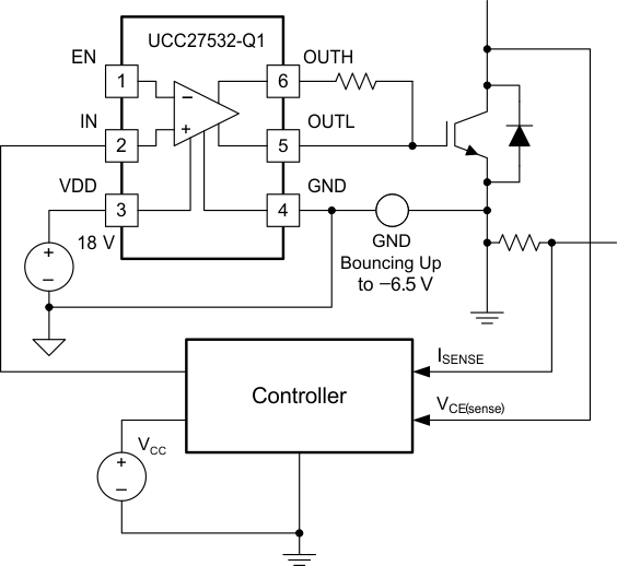
UCC27532-Q1 Driving IGBT Without Negative Bias Driving IGBT Without Negative Bias