SLUSBD9A February 2013 – September 2024 UCC27532
PRODUCTION DATA
- 1
- 1 Features
- 2 Applications
- 3 Description
- 4 Pin Configuration and Functions
- 5 Specifications
- 6 Detailed Description
- 7 Application and Implementation
- 8 Layout
- 9 Device and Documentation Support
- 10Revision History
- 11Mechanical, Packaging, and Orderable Information
Package Options
Refer to the PDF data sheet for device specific package drawings
Mechanical Data (Package|Pins)
- DBV|6
Thermal pad, mechanical data (Package|Pins)
Orderable Information
5.4 Electrical Characteristics
Unless otherwise noted, VDD = 18 V, TA = TJ = -40°C to 140°C, IN switching from 0 V to VDD, 1-µF capacitor from VDD to GND, f = 100 kHz. Currents are positive into, negative out of the specified terminal. OUTH and OUTL are tied together. Typical condition specifications are at 25°C.
| PARAMETER | CONDITION | MIN | TYP | MAX | UNITS | |
|---|---|---|---|---|---|---|
| Bias Currents | ||||||
| IDDoff | Startup Current, VDD = 7.0 | IN, EN = VDD | 100 | 240 | 350 | μA |
| IN, EN = GND | 100 | 250 | 350 | |||
| Under Voltage Lockout (UVLO) | ||||||
| VON | Supply start threshold | 8.0 | 8.9 | 9.8 | V | |
| VOFF | Minimum operating voltage after supply start | 7.3 | 8.2 | 9.1 | ||
| VDD_H | Supply voltage hysteresis | 0.7 | ||||
| Input (IN) | ||||||
| VIN_H | Input signal high threshold | VDD = 16V, Output high | 8.8 | 9.4 | 10 | V |
| VIN_L | Input signal low threshold | VDD = 16V, Output low | 6.7 | 7.3 | 7.9 | |
| VIN_HYS | Input signal hysteresis | VDD = 16V | 2.1 | |||
| Enable (EN) | ||||||
| VEN_H | Enable signal high threshold | VDD = 16V, Output high | 1.7 | 1.9 | 2.1 | V |
| VEN_L | Enable signal low threshold | VDD = 16V, Output low | 0.8 | 1.0 | 1.2 | |
| VEN_HYS | Enable signal hysteresis | VDD = 16V | 0.9 | |||
| Outputs (OUTH/OUTL) | ||||||
| ISRC/SNK | Source peak current (OUTH)/ sink peak current (OUTL)(13)(1) | CLOAD = 0.22 µF, f = 1 kHz | -2.5/+5 | A | ||
| VOH | OUTH, high voltage | IOUTH = -10 mA | VDD -0.2 | VDD -0.12 | VDD -0.07 | V |
| VOL | OUTL, low voltage | IOUTL = 100 mA | 0.065 | 0.125 | ||
| ROH | OUTH, pull-up resistance (15)(3) | TA = 25°C, IOUT = -10 mA | 11 | 12 | 12.5 | Ω |
| TA = -40°C to 140°C, IOUT = -10 mA | 7 | 12 | 20 | |||
| ROL | OUTL, pull-down resistance | TA = 25°C, IOUT = 100 mA | 0.45 | 0.65 | 0.85 | |
| TA = -40°C to 140°C, IOUT = 100 mA | 0.3 | 0.65 | 1.25 | |||
| Switching Time (1)(2) | ||||||
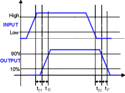
| tR | Rise time | CLOAD = 1.8 nF | 15 | ns | ||
| tF | Fall time | CLOAD = 1.8 nF | 7 | |||
| tD1 | Turn-on propagation delay | CLOAD = 1.8 nF, IN = 0 V to VDD | 17 | 26 | ||
| tD2 | Turn-off propagation delay | CLOAD = 1.8 nF, IN = VDD to 0 V | 17 | 26 | ||
(1) Ensured by design and tested during characterization. Not production tested.
(2) See Figure 5-1.
(3) Output pull-up resistance here is a DC measurement that measures resistance of PMOS structure only, not N-channel structure. The effective dynamic pull-up resistance is 3 x ROL.
 Figure 5-1 Timing Diagram (OUTH tied to OUTL)(Input = IN,
Output = OUT (EN = VDD), or Input = EN, Output = OUT (IN = VDD)