SLUSBD9A February 2013 – September 2024 UCC27532
PRODUCTION DATA
- 1
- 1 Features
- 2 Applications
- 3 Description
- 4 Pin Configuration and Functions
- 5 Specifications
- 6 Detailed Description
- 7 Application and Implementation
- 8 Layout
- 9 Device and Documentation Support
- 10Revision History
- 11Mechanical, Packaging, and Orderable Information
Package Options
Refer to the PDF data sheet for device specific package drawings
Mechanical Data (Package|Pins)
- DBV|6
Thermal pad, mechanical data (Package|Pins)
Orderable Information
5.5 Typical Characteristics
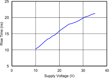 Figure 5-2 Rise Time vs Supply
Voltage
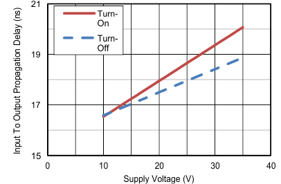 Figure 5-4 Propagation Delay vs
Supply Voltage
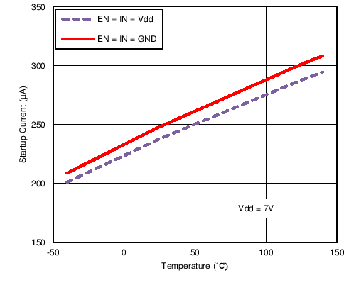 Figure 5-6 Start-Up Current vs
Temperature
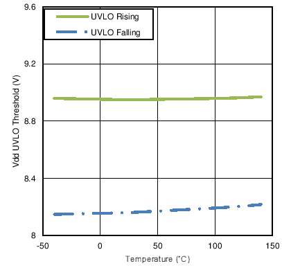 Figure 5-8 UVLO Threshold Voltage vs
Temperature
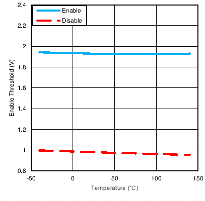 Figure 5-10 Enable Threshold vs
Temperature
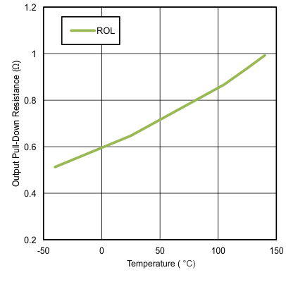 Figure 5-12 Output Pull-Down
Resistance vs Temperature
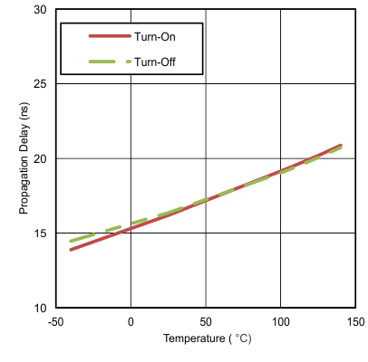 Figure 5-14 Input-to-Output
Propagation Delay vs Temperature
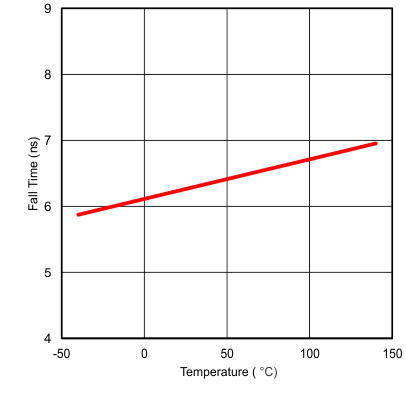 Figure 5-16 Fall Time vs
Temperature
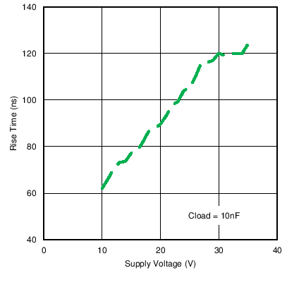 Figure 5-18 Rise Time vs Supply
Voltage
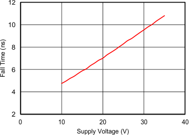 Figure 5-3 Fall Time vs Supply
Voltage
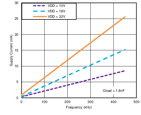 Figure 5-5 Operating Supply Current
vs Frequency
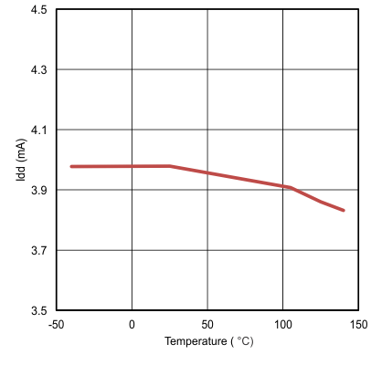 Figure 5-7 Operating Supply Current
vs Temperature (output switching)
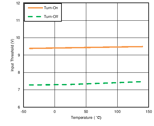 Figure 5-9 Input Threshold vs
Temperature
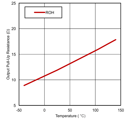 Figure 5-11 Output Pull-Up Resistance
vs Temperature
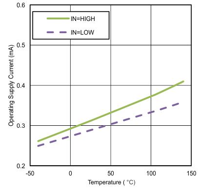 Figure 5-13 Operating Supply Current
vs Temperature (output in DC on/off condition)
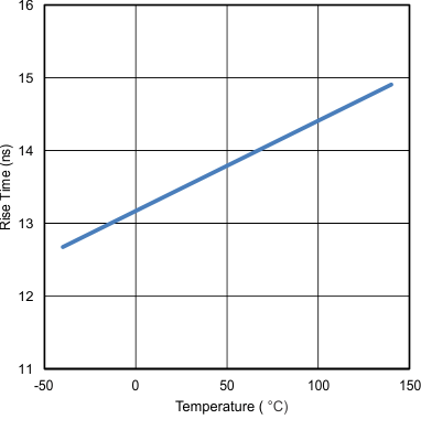 Figure 5-15 Rise Time vs
Temperature
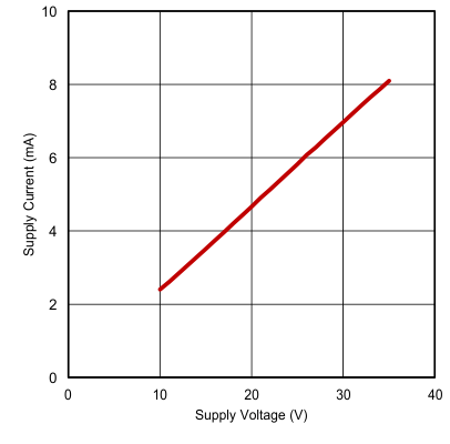 Figure 5-17 Operating Supply Current
vs Supply Voltage (output switching)
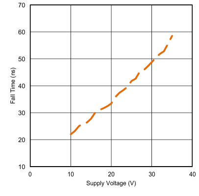 Figure 5-19 Fall Time vs Supply
Voltage