SLUSBD9A February 2013 – September 2024 UCC27532
PRODUCTION DATA
- 1
- 1 Features
- 2 Applications
- 3 Description
- 4 Pin Configuration and Functions
- 5 Specifications
- 6 Detailed Description
- 7 Application and Implementation
- 8 Layout
- 9 Device and Documentation Support
- 10Revision History
- 11Mechanical, Packaging, and Orderable Information
Package Options
Refer to the PDF data sheet for device specific package drawings
Mechanical Data (Package|Pins)
- DBV|6
Thermal pad, mechanical data (Package|Pins)
Orderable Information
6.2.1 VDD Under Voltage Lockout
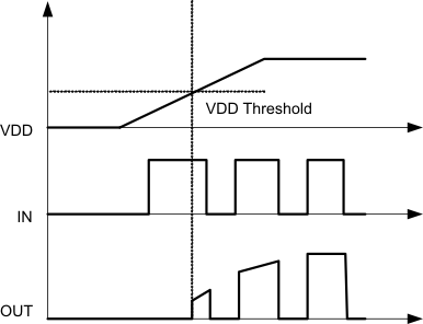
The UCC27532 device has internal under voltage lockout (UVLO) protection feature on the VDD pin supply circuit blocks. To ensure acceptable power dissipation in the power switch, this UVLO prevents the operation of the gate driver at low supply voltages. Whenever the driver is in UVLO condition (when VDD voltage less than VON during power-up and when VDD voltage is less than VOFF during power down), this circuit holds all outputs LOW, regardless of the status of the inputs. The UVLO is typically 8.9 V with 700-mV typical hysteresis. This hysteresis helps prevent chatter when low VDD supply voltages have noise from the power supply and also when there are droops in the VDD bias voltage when the system commences switching and there is a sudden increase in IDD. The capability to operate at voltage levels such as 10 V to 32 V provides flexibility to drive Si MOSFETs, IGBTs, and emerging SiC FETs.
 Figure 6-1 Power Up