SLUSBY6B August 2015 – March 2017 UCC27714
PRODUCTION DATA.
- 1 Features
- 2 Applications
- 3 Description
- 4 Revision History
- 5 Pin Configuration and Functions
- 6 Specifications
- 7 Detailed Description
-
8 Application and Implementation
- 8.1 Application Information
- 8.2
Typical Application
- 8.2.1 Design Requirements
- 8.2.2
Detailed Design Procedure
- 8.2.2.1 Selecting HI and LI Low Pass Filter Components (RHI, RLI, CHI, CLI)
- 8.2.2.2 Selecting Bootstrap Capacitor (CBOOT)
- 8.2.2.3 Selecting VDD Bypass/Holdup Capacitor (CVDD) and Rbias
- 8.2.2.4 Selecting Bootstrap Resistor (RBOOT)
- 8.2.2.5 Selecting Gate Resistor RHO/RLO
- 8.2.2.6 Selecting Bootstrap Diode
- 8.2.2.7 Estimate the UCC27714 Power Losses (PUCC27714)
- 8.2.2.8 Application Example Schematic Note
- 8.2.2.9 LO and HO Overshoot and Undershoot
- 8.2.3 Application Curves
- 9 Power Supply Recommendations
- 10Layout
- 11Device and Documentation Support
- 12Mechanical, Packaging, and Orderable Information
- 13Mechanical, Packaging, and Orderable Information
Package Options
Mechanical Data (Package|Pins)
- D|14
Thermal pad, mechanical data (Package|Pins)
Orderable Information
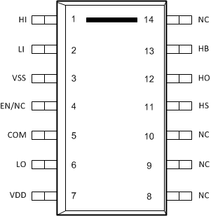
5 Pin Configuration and Functions
D Package
14-Pin SOIC
Top View

Pin Functions
| PIN | I/O | DESCRIPTION | |
|---|---|---|---|
| NAME | NO. | ||
| COM | 5 | – | Return for low-side driver output. |
| EN/NC | 4 | I | Enable input for high-side and low-side driver. This pin biased LOW, disables both HO and LO regardless of HI and LI state, This pin biased high or floating enables both HO and LO. |
| HB | 13 | I | High-side floating supply. Bypass this pin to HS with a suitable capacitor to sustain boot-strap circuit operation in the desired application, typically 10× bigger than gate capacitance. |
| HI | 1 | I | Logic input for high-side driver. If HI is unbiased or floating, HO is held low. |
| HO | 12 | O | High-side driver output. |
| HS | 11 | – | Return for high-side floating supply. |
| LI | 2 | I | Logic input for low-side driver. If LI is unbiased or floating, LO is held low. |
| LO | 6 | O | Low-side driver output. |
| NC | 8, 9, 10, 14 | – | No connection. |
| VDD | 7 | I | Bias supply input. Power supply for the input logic side of the device and also low-side driver output. Bypass this pin to VSS with typical 1-µF SMD capacitor (typically CVDD needs to be 10 × CBOOT). If shunt resistor used between COM and VSS, then also bypass this pin to COM with 1-µF SMD capacitor. |
| VSS | 3 | – | Logic ground. |