SGLS121D December 2002 – June 2020 UCC2800-Q1 , UCC2801-Q1 , UCC2802-Q1 , UCC2803-Q1 , UCC2804-Q1 , UCC2805-Q1
PRODUCTION DATA.
- 1 Features
- 2 Applications
- 3 Description
- 4 Revision History
- 5 Description (continued)
- 6 Device Comparison Table
- 7 Pin Configuration and Functions
- 8 Specifications
-
9 Detailed Description
- 9.1 Overview
- 9.2 Functional Block Diagram
- 9.3
Feature Description
- 9.3.1 Detailed Pin Description
- 9.3.2 Undervoltage Lockout (UVLO)
- 9.3.3 Self-Biasing, Active Low Output
- 9.3.4 Reference Voltage
- 9.3.5 Oscillator
- 9.3.6 Synchronization
- 9.3.7 PWM Generator
- 9.3.8 Minimum Off-Time Setting (Dead-Time Control)
- 9.3.9 Leading Edge Blanking
- 9.3.10 Minimum Pulse Width
- 9.3.11 Current Limiting
- 9.3.12 Overcurrent Protection and Full Cycle Restart
- 9.3.13 Soft Start
- 9.3.14 Slope Compensation
- 9.4 Device Functional Modes
- 10Application and Implementation
- 11Power Supply Recommendations
- 12Layout
- 13Device and Documentation Support
- 14Mechanical, Packaging, and Orderable Information
Package Options
Refer to the PDF data sheet for device specific package drawings
Mechanical Data (Package|Pins)
- D|8
Thermal pad, mechanical data (Package|Pins)
Orderable Information
11 Power Supply Recommendations
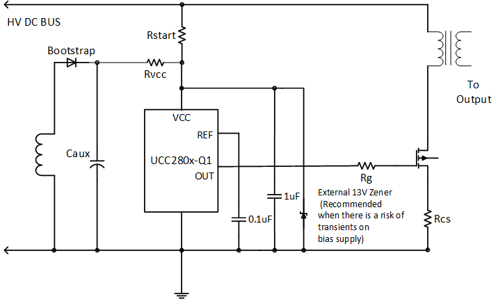
An internal VCC shunt regulator is incorporated in each member of the UCC280x-Q1PWMs to regulate the supply voltage at approximately 13.5 V. A series resistor from VCC to the input supply source is required with inputs above 12 V to limit the shunt regulator current. A maximum of 10 mA can be shunted to ground by the internal regulator. The internal regulator in conjunction with the device’s low start-up and operating current can greatly simplify powering the device and may eliminate the requirement for a regulated bootstrap auxiliary supply and winding in many applications. The supply voltage is MOSFET gate level compatible and requires no external Zener diode or regulator protection with a current-limited input supply. The UVLO start-up threshold is 1 V below the shunt regulator level on the UCC2802-Q1 and UCC2804-Q1 devices to ensure start-up. It is important to bypass the ICs supply (VCC) and reference voltage (REF) pins with a 0.1-µF to 1-µF ceramic capacitor to ground. The capacitors must be placed as close to the actual pin connections as possible for optimal noise filtering. A second, larger filter capacitor may also be required in offline applications to hold the supply voltage (VCC) above the UVLO turnoff threshold during start-up.
The UVLO start threshold of the UCC280-[2,4]-Q1 devices has a range of 11.5 V to 13.5 V, while the protection zener voltage can vary from 12 V to 15 V. However, the absolute maximum supply voltage of the IC is specified at 12 V. This absolute maximum is defined as the lowest possible Zener voltage when driven from a low impedance (voltage) source. The zener voltage is always higher than the UVLO start voltage. These two parameters track each other and the chip is tested to guarantee that the Zener voltage will never be below that of the start voltage. To limit the current flowing in the internal clamp zener, a series resistor must be added. Failure to provide a series resistance between the auxiliary voltage source and the Vcc pin of the controller, to limit the current and voltage stress within rated levels on the Vcc pin may result in permanent damage to the controller. In automotive or industrial applications where there is a risk of high power load transients which may cause transients or voltage excursions on the Vcc rail supplying the PWM controller it is recommended to add an external Zener diode across the Vcc pin. The external Zener acts as an additional protection to the impedance provided by the series resistor between the Vcc source and Vcc pin.
Placing a resistor, Rg, in series with the gate of the mosfet allows the mosfet switching speed to be adjusted and also can be used to keep the peak gate drive currents within the specified limits of the controller.
 Figure 43. Different Ways of Powering Up the Device