SGLS121D December 2002 – June 2020 UCC2800-Q1 , UCC2801-Q1 , UCC2802-Q1 , UCC2803-Q1 , UCC2804-Q1 , UCC2805-Q1
PRODUCTION DATA.
- 1 Features
- 2 Applications
- 3 Description
- 4 Revision History
- 5 Description (continued)
- 6 Device Comparison Table
- 7 Pin Configuration and Functions
- 8 Specifications
-
9 Detailed Description
- 9.1 Overview
- 9.2 Functional Block Diagram
- 9.3
Feature Description
- 9.3.1 Detailed Pin Description
- 9.3.2 Undervoltage Lockout (UVLO)
- 9.3.3 Self-Biasing, Active Low Output
- 9.3.4 Reference Voltage
- 9.3.5 Oscillator
- 9.3.6 Synchronization
- 9.3.7 PWM Generator
- 9.3.8 Minimum Off-Time Setting (Dead-Time Control)
- 9.3.9 Leading Edge Blanking
- 9.3.10 Minimum Pulse Width
- 9.3.11 Current Limiting
- 9.3.12 Overcurrent Protection and Full Cycle Restart
- 9.3.13 Soft Start
- 9.3.14 Slope Compensation
- 9.4 Device Functional Modes
- 10Application and Implementation
- 11Power Supply Recommendations
- 12Layout
- 13Device and Documentation Support
- 14Mechanical, Packaging, and Orderable Information
Package Options
Refer to the PDF data sheet for device specific package drawings
Mechanical Data (Package|Pins)
- D|8
Thermal pad, mechanical data (Package|Pins)
Orderable Information
9.3.6 Synchronization
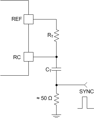
Synchronization of these PWM controllers is best obtained by the universal technique shown in Figure 19. The ICs oscillator is programmed to free run at a frequency about 20% lower than that of the synchronizing frequency. A brief positive pulse is applied across the 50-Ω resistor to force synchronization. Typically, a 1-V amplitude pulse of 100-ns width is sufficient for most applications.
The ICs can also be synchronized to a pulse train input directly to the oscillator RC pin. Note that the IC internally pulls low at this node once the upper oscillator threshold is crossed. This 130-Ω impedance to ground remains active until the pin is lowered to approximately 0.2 V. External synchronization circuits must accommodate these conditions.
 Figure 19. Synchronizing the Oscillator