SLUSD37E October   2017  – November 2019 UCC28056

PRODUCTION DATA.  

  1. Features
  2. Applications
  3. Description
    1.     No Load Power
      1.      Device Images
        1.       Simplified Application
  4. Revision History
  5. Device Comparison Tables
  6. Pin Configuration and Functions
    1.     Pin Functions
  7. Specifications
    1. 7.1 Absolute Maximum Ratings
    2. 7.2 ESD Ratings
    3. 7.3 Recommended Operating Conditions
    4. 7.4 Thermal Information
    5. 7.5 Electrical Characteristics
    6. 7.6 Typical Characteristics
  8. Detailed Description
    1. 8.1 Overview
    2. 8.2 Functional Block Diagram
    3. 8.3 Feature Description
      1. 8.3.1 CrM/DCM Control Principle
      2. 8.3.2 Line Voltage Feed-Forward
        1. 8.3.2.1 Peak Line Voltage Detection
      3. 8.3.3 Valley Switching and CrM/DCM Hysteresis
        1. 8.3.3.1 Valley Delay Adjustment
      4. 8.3.4 Transconductance Amplifier with Transient Speed-up Function
      5. 8.3.5 Faults and Protections
        1. 8.3.5.1 Supply Undervoltage Lockout
        2. 8.3.5.2 Two Level Over-Current Protection
          1. 8.3.5.2.1 Cycle-by-Cycle Current Limit Ocp1
          2. 8.3.5.2.2 Ocp2 Gross Over-Current or CCM Protection
        3. 8.3.5.3 Output Over-Voltage Protection
          1. 8.3.5.3.1 First Level Output Over-Voltage Protection (Ovp1)
          2. 8.3.5.3.2 Second Level Over-Voltage Protection (Ovp2)
        4. 8.3.5.4 Thermal Shutdown Protection
        5. 8.3.5.5 Line Under-Voltage or Brown-In
      6. 8.3.6 High-Current Driver
    4. 8.4 Controller Functional Modes
      1. 8.4.1 Burst Mode Operation
      2. 8.4.2 Soft Start
  9. Application and Implementation
    1. 9.1 Application Information
    2. 9.2 Typical Application
      1. 9.2.1 Design Requirements
      2. 9.2.2 Detailed Design Procedure
        1. 9.2.2.1 Custom Design With WEBENCH® Tools
        2. 9.2.2.2 Power Stage Design
          1. 9.2.2.2.1 Boost Inductor Design
          2. 9.2.2.2.2 Boost Switch Selection
          3. 9.2.2.2.3 Boost Diode Selection
          4. 9.2.2.2.4 Output Capacitor Selection
        3. 9.2.2.3 ZCD/CS Pin
          1. 9.2.2.3.1 Voltage Spikes on the ZCD/CS pin Waveform
        4. 9.2.2.4 VOSNS Pin
        5. 9.2.2.5 Voltage Loop Compensation
          1. 9.2.2.5.1 Plant Model
          2. 9.2.2.5.2 Compensator Design
      3. 9.2.3 Application Curves
  10. 10Power Supply Recommendations
  11. 11Layout
    1. 11.1 Layout Guidelines
      1. 11.1.1 VOSNS Pin
      2. 11.1.2 ZCD/CS Pin
      3. 11.1.3 VCC Pin
      4. 11.1.4 GND Pin
      5. 11.1.5 DRV Pin
      6. 11.1.6 COMP Pin
    2. 11.2 Layout Example
  12. 12Device and Documentation Support
    1. 12.1 Custom Design With WEBENCH® Tools
    2. 12.2 Receiving Notification of Documentation Updates
    3. 12.3 Community Resources
    4. 12.4 Trademarks
    5. 12.5 Electrostatic Discharge Caution
    6. 12.6 Glossary
  13. 13Mechanical, Packaging, and Orderable Information

Package Options

Mechanical Data (Package|Pins)
Thermal pad, mechanical data (Package|Pins)
Orderable Information

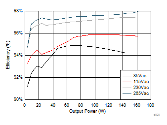
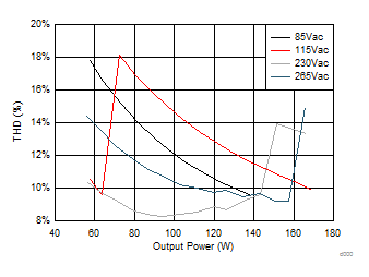
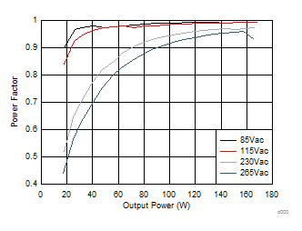
Application Curves

UCC28056 d00021_SLUSD73.gif
Figure 33. Efficiency vs Output Power
UCC28056 d00023_SLUSD73.gif
Figure 35. THD vs Output Power
UCC28056 d00022_SLUSD73.gif
Figure 34. Power Factor vs Output Power