SLUSD37E October 2017 – November 2019 UCC28056
PRODUCTION DATA.
- 1 Features
- 2 Applications
- 3 Description
- 4 Revision History
- 5 Device Comparison Tables
- 6 Pin Configuration and Functions
- 7 Specifications
-
8 Detailed Description
- 8.1 Overview
- 8.2 Functional Block Diagram
- 8.3
Feature Description
- 8.3.1 CrM/DCM Control Principle
- 8.3.2 Line Voltage Feed-Forward
- 8.3.3 Valley Switching and CrM/DCM Hysteresis
- 8.3.4 Transconductance Amplifier with Transient Speed-up Function
- 8.3.5 Faults and Protections
- 8.3.6 High-Current Driver
- 8.4 Controller Functional Modes
- 9 Application and Implementation
- 10Power Supply Recommendations
- 11Layout
- 12Device and Documentation Support
- 13Mechanical, Packaging, and Orderable Information
Package Options
Mechanical Data (Package|Pins)
- DBV|6
Thermal pad, mechanical data (Package|Pins)
Orderable Information
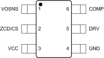
6 Pin Configuration and Functions
DBV Package
6-Pin SOT-23
Top View

Pin Functions
| PIN | I/O | DESCRIPTION | |
|---|---|---|---|
| NAME | NO. | ||
| COMP | 6 | I/O | Output of the internal transconductance error amplifier and power demand input. To achieve compensation of the voltage loop, connect a suitable RC network from this pin to GND. The error amplifier output is internally limited to VCOClmp. An internal resistor, RCODisch, discharges the external compensation network when the controller is in its Stopb state or when the Ovp2 comparator is tripped. Switching stops, and the controller enters a low-power state (BstOffb), when the voltage on the COMP pin drops below VBSTFall. Switching resumes when the COMP pin voltage exceeds VBSTRise. |
| DRV | 5 | I/O | GATE connection to drive the main power MOSFET. This output is internally limited to VDRHigh. This is done to reduce power dissipation in the internal driver and allow controller operation from high VCC voltages. An external resistor connected from DRV to GND adjusts the delay between the Drain waveform falling below VIn and the DRV rising edge, allowing the turn on transition to be aligned to the valley minimum accurately over a wide range of idle ring oscillating frequency. |
| GND | 4 | G | Controller Ground reference pin. Connect to the power stage at the lower terminal of the current sense resistor, RCS, only. |
| VCC | 3 | P | Positive supply voltage. Switching operation can start once VCC exceeds VCCStart. Switching operation ceases if VCC drops below VCCStop for longer than TUVLOBlk. |
| ZCD/CS | 2 | I | This pin is fed by a potential divider connected across the Drain & Source pins of the power MOSFET switch. While the DRV pin is high this pin monitors the voltage across the current sense resistor, RCS. This pin implement over-current protection functions. While the DRV pin in low this pin monitors the Drain voltage waveform. Input voltage applied to the power stage can be obtained by filtering the Drain waveform. Input voltage provides Line voltage feed - forward and Line Brown - In features. Drain voltage waveform is also used to provide ZCD detection, valley synchronization and second level output over - voltage protection features. |
| VOSNS | 1 | I | Voltage error amplifier inverting input. The error amplifier non - inverting input connects to internal reference voltage VOSReg. Error amplifier gain increases with error magnitude to improve transient response without compromising Line current distortion. Output over-voltage protection is implemented on this pin. Switching operation halts if the voltage on this pin exceeds VOvp1Rise and resumes when it drops below VOvp1Fall. |