SLUSAO7C September 2011 – July 2024 UCC28063
PRODUCTION DATA
- 1
- 1 Features
- 2 Applications
- 3 Description
- 4 Revision History
- 5 Pin Configuration and Functions
- 6 Specifications
-
7 Detailed Description
- 7.1 Overview
- 7.2 Functional Block Diagram
- 7.3
Feature Description
- 7.3.1 Principles of Operation
- 7.3.2 Natural Interleaving
- 7.3.3 On-Time Control, Maximum Frequency Limiting, and Restart Timer
- 7.3.4 Distortion Reduction
- 7.3.5 Zero-Current Detection and Valley Switching
- 7.3.6 Phase Management and Light-Load Operation
- 7.3.7 External Disable
- 7.3.8 Improved Error Amplifier
- 7.3.9 Soft Start
- 7.3.10 Brownout Protection
- 7.3.11 Dropout Detection
- 7.3.12 VREF
- 7.3.13 VCC
- 7.3.14 Control of Downstream Converter
- 7.3.15
System Level Protections
- 7.3.15.1 Failsafe OVP - Output Overvoltage Protection
- 7.3.15.2 Overcurrent Protection
- 7.3.15.3 Open-Loop Protection
- 7.3.15.4 VCC Undervoltage Lock-Out (UVLO) Protection
- 7.3.15.5 Phase-Fail Protection
- 7.3.15.6 CS-Open, TSET-Open and -Short Protection
- 7.3.15.7 Thermal Shutdown Protection
- 7.3.15.8 AC-Line Brownout and Dropout Protections
- 7.3.15.9 Fault Logic Diagram
- 7.4 Device Functional Modes
-
8 Applications and Implementation
- 8.1 Application Information
- 8.2
Typical Application
- 8.2.1 Design Requirements
- 8.2.2
Detailed Design Procedure
- 8.2.2.1 Inductor Selection
- 8.2.2.2 ZCD Resistor Selection (RZA, RZB)
- 8.2.2.3 HVSEN
- 8.2.2.4 Output Capacitor Selection
- 8.2.2.5 Selecting (RS) For Peak Current Limiting
- 8.2.2.6 Power Semiconductor Selection (Q1, Q2, D1, D2)
- 8.2.2.7 Brownout Protection
- 8.2.2.8 Converter Timing
- 8.2.2.9 Programming VOUT
- 8.2.2.10 Voltage Loop Compensation
- 8.2.3 Application Curves
- 9 Power Supply Recommendations
- 10Layout
- 11Device and Documentation Support
- 12Mechanical, Packaging, and Orderable Information
Package Options
Mechanical Data (Package|Pins)
- D|16
Thermal pad, mechanical data (Package|Pins)
Orderable Information
8.2.2.10 Voltage Loop Compensation
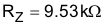
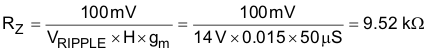
Resistor RZ is sized to attenuate low-frequency ripple to less than 2% of the voltage amplifier output range. This value ensures good power factor and low harmonic distortion on the input current.
The transconductance amplifier small-signal gain is shown in Equation 56:

The voltage-divider feedback gain is shown in Equation 57:
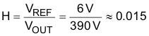
The value of RZ is calculated as shown in Equation 58:
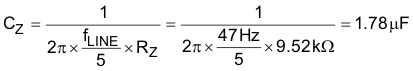
CZ is then set to add 45° phase margin at 1/5th of the line frequency, as shown in Equation 59:
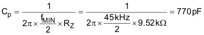
CP is sized to attenuate high-frequency switching noise, as shown in Equation 60:
Standard values should be chosen for RZ, CZ and CP, as shown in Equation 61 to Equation 63.