SLUSAO7C September 2011 – July 2024 UCC28063
PRODUCTION DATA
- 1
- 1 Features
- 2 Applications
- 3 Description
- 4 Revision History
- 5 Pin Configuration and Functions
- 6 Specifications
-
7 Detailed Description
- 7.1 Overview
- 7.2 Functional Block Diagram
- 7.3
Feature Description
- 7.3.1 Principles of Operation
- 7.3.2 Natural Interleaving
- 7.3.3 On-Time Control, Maximum Frequency Limiting, and Restart Timer
- 7.3.4 Distortion Reduction
- 7.3.5 Zero-Current Detection and Valley Switching
- 7.3.6 Phase Management and Light-Load Operation
- 7.3.7 External Disable
- 7.3.8 Improved Error Amplifier
- 7.3.9 Soft Start
- 7.3.10 Brownout Protection
- 7.3.11 Dropout Detection
- 7.3.12 VREF
- 7.3.13 VCC
- 7.3.14 Control of Downstream Converter
- 7.3.15
System Level Protections
- 7.3.15.1 Failsafe OVP - Output Overvoltage Protection
- 7.3.15.2 Overcurrent Protection
- 7.3.15.3 Open-Loop Protection
- 7.3.15.4 VCC Undervoltage Lock-Out (UVLO) Protection
- 7.3.15.5 Phase-Fail Protection
- 7.3.15.6 CS-Open, TSET-Open and -Short Protection
- 7.3.15.7 Thermal Shutdown Protection
- 7.3.15.8 AC-Line Brownout and Dropout Protections
- 7.3.15.9 Fault Logic Diagram
- 7.4 Device Functional Modes
-
8 Applications and Implementation
- 8.1 Application Information
- 8.2
Typical Application
- 8.2.1 Design Requirements
- 8.2.2
Detailed Design Procedure
- 8.2.2.1 Inductor Selection
- 8.2.2.2 ZCD Resistor Selection (RZA, RZB)
- 8.2.2.3 HVSEN
- 8.2.2.4 Output Capacitor Selection
- 8.2.2.5 Selecting (RS) For Peak Current Limiting
- 8.2.2.6 Power Semiconductor Selection (Q1, Q2, D1, D2)
- 8.2.2.7 Brownout Protection
- 8.2.2.8 Converter Timing
- 8.2.2.9 Programming VOUT
- 8.2.2.10 Voltage Loop Compensation
- 8.2.3 Application Curves
- 9 Power Supply Recommendations
- 10Layout
- 11Device and Documentation Support
- 12Mechanical, Packaging, and Orderable Information
Package Options
Mechanical Data (Package|Pins)
- D|16
Thermal pad, mechanical data (Package|Pins)
Orderable Information
7.3.10 Brownout Protection
As the power line RMS voltage decreases, RMS input current must increase to maintain a constant output voltage for a specific load. Brownout protection helps prevent excess system thermal stress (due to the higher RMS input current) from exceeding a safe operating level. Power-line voltage is sensed at VINAC. When the VINAC fails to exceed the brownout threshold for the brownout filter time, a brownout condition is detected and both gate drive outputs are turned off. During brownout, COMP is actively pulled low and a soft-start condition is initiated. Hysteresis is built into the brownout detection circuit to avoid chatter around the threshold. When VINAC rises above the brownout threshold, the power stage soft-starts as COMP rises with controlled current.
The brownout detection threshold and its hysteresis are set by the voltage-divider ratio and resistor values. Brownout protection is based on VINAC peak voltage; the threshold and hysteresis are also based on the line peak voltage. Major hysteresis is provided by a 2-μA current-sink (IBOHYS) enabled whenever VINAC falls below the brownout detection threshold. Minor hysteresis is also present in the form of a 50-mV offset (VBOHYS) between the VINAC detection and clear thresholds. The peak VINAC voltage can be easily translated into an RMS value. Example resistor values for the voltage divider are 8.61 MΩ ±1% from the rectified input voltage to VINAC and 133 kΩ ±1% from VINAC to ground. These resistors set the typical thresholds for RMS line voltages, as shown in Table 7-1.
| THRESHOLD | AC-LINE VOLTAGE (RMS) |
|---|---|
| Falling | 66 V |
| Rising | 78 V |
Equation 8 and Equation 9 can be used to calculate the VINAC divider-resistor values based on desired brownout detection and brownout clear voltage levels. VAC_OK is the desired RMS turn-on voltage, VAC_BO is the desired RMS turn-off brownout voltage, and VLOSS is total series voltage drop due to wiring, EMI-filter, and bridge-rectifier impedances at VAC_BO. VBODET, VBOHYS and IBOHYS are found in the data-tables of this datasheet.
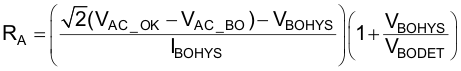
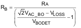
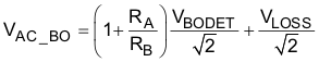
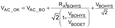
Once standard values for the VINAC divider-resistors RA and RB are selected, the actual turn-on and brownout threshold RMS voltages for the ac-line can be back-calculated with Equation 10 and Equation 11:
An example of the timing for the brownout function is illustrated in Figure 7-7.
For a quick estimation of the turn-on and brownout voltages, simplify the foregoing equations by setting the VLOSS and VBOHYS terms to zero.