SLUSAO7C September 2011 – July 2024 UCC28063
PRODUCTION DATA
- 1
- 1 Features
- 2 Applications
- 3 Description
- 4 Revision History
- 5 Pin Configuration and Functions
- 6 Specifications
-
7 Detailed Description
- 7.1 Overview
- 7.2 Functional Block Diagram
- 7.3
Feature Description
- 7.3.1 Principles of Operation
- 7.3.2 Natural Interleaving
- 7.3.3 On-Time Control, Maximum Frequency Limiting, and Restart Timer
- 7.3.4 Distortion Reduction
- 7.3.5 Zero-Current Detection and Valley Switching
- 7.3.6 Phase Management and Light-Load Operation
- 7.3.7 External Disable
- 7.3.8 Improved Error Amplifier
- 7.3.9 Soft Start
- 7.3.10 Brownout Protection
- 7.3.11 Dropout Detection
- 7.3.12 VREF
- 7.3.13 VCC
- 7.3.14 Control of Downstream Converter
- 7.3.15
System Level Protections
- 7.3.15.1 Failsafe OVP - Output Overvoltage Protection
- 7.3.15.2 Overcurrent Protection
- 7.3.15.3 Open-Loop Protection
- 7.3.15.4 VCC Undervoltage Lock-Out (UVLO) Protection
- 7.3.15.5 Phase-Fail Protection
- 7.3.15.6 CS-Open, TSET-Open and -Short Protection
- 7.3.15.7 Thermal Shutdown Protection
- 7.3.15.8 AC-Line Brownout and Dropout Protections
- 7.3.15.9 Fault Logic Diagram
- 7.4 Device Functional Modes
-
8 Applications and Implementation
- 8.1 Application Information
- 8.2
Typical Application
- 8.2.1 Design Requirements
- 8.2.2
Detailed Design Procedure
- 8.2.2.1 Inductor Selection
- 8.2.2.2 ZCD Resistor Selection (RZA, RZB)
- 8.2.2.3 HVSEN
- 8.2.2.4 Output Capacitor Selection
- 8.2.2.5 Selecting (RS) For Peak Current Limiting
- 8.2.2.6 Power Semiconductor Selection (Q1, Q2, D1, D2)
- 8.2.2.7 Brownout Protection
- 8.2.2.8 Converter Timing
- 8.2.2.9 Programming VOUT
- 8.2.2.10 Voltage Loop Compensation
- 8.2.3 Application Curves
- 9 Power Supply Recommendations
- 10Layout
- 11Device and Documentation Support
- 12Mechanical, Packaging, and Orderable Information
Package Options
Mechanical Data (Package|Pins)
- D|16
Thermal pad, mechanical data (Package|Pins)
Orderable Information
8.2.2.6 Power Semiconductor Selection (Q1, Q2, D1, D2)
The selection of Q1, Q2, D1, and D2 are based on the power requirements of the design. Application Note SLUU138, UCC38050 100-W Critical Conduction Power Factor Corrected (PFC) Pre-regulator, explains how to select power semiconductor components for transition-mode PFC pre-regulators.
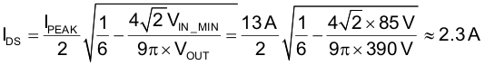
The MOSFET (Q1, Q2) pulsed-drain maximum current is shown in Equation 41:

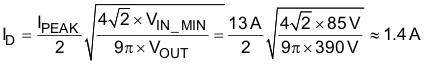
The MOSFET (Q1, Q2) RMS current calculation is shown in Equation 42:
To meet the power requirements of the design, IRFB11N50A 500-V MOSFETs were chosen for Q1 and Q2.
The boost diode (D1, D2) RMS current is shown in Equation 43:
To meet the power requirements of the design, MURS360T3, 600-V diodes were chosen for D1 and D2.