SNVSA88C December 2014 – November 2016 UCC28063A
PRODUCTION DATA.
- 1 Features
- 2 Applications
- 3 Description
- 4 Revision History
- 5 Description (Continued)
- 6 Pin Configuration and Functions
- 7 Specifications
-
8 Detailed Description
- 8.1 Overview
- 8.2 Functional Block Diagram
- 8.3
Feature Description
- 8.3.1 Principles of Operation
- 8.3.2 Natural Interleaving
- 8.3.3 On-Time Control, Maximum Frequency Limiting, and Restart Timer
- 8.3.4 Distortion Reduction
- 8.3.5 Zero-Current Detection and Valley Switching
- 8.3.6 Phase Management and Light-Load Operation
- 8.3.7 External Disable
- 8.3.8 Improved Error Amplifier
- 8.3.9 Soft Start
- 8.3.10 Brownout Protection
- 8.3.11 Dropout Detection
- 8.3.12 VREF
- 8.3.13 VCC
- 8.3.14 Control of Downstream Converter
- 8.3.15
System Level Protections
- 8.3.15.1 Failsafe OVP - Output Overvoltage Protection
- 8.3.15.2 Overcurrent Protection
- 8.3.15.3 Open-Loop Protection
- 8.3.15.4 VCC Undervoltage Lock-Out (UVLO) Protection
- 8.3.15.5 Phase-Fail Protection
- 8.3.15.6 Thermal Shutdown Protection
- 8.3.15.7 AC-Line Brownout and Dropout Protections
- 8.3.15.8 Fault Logic Diagram
- 8.4 Device Functional Modes
-
9 Applications and Implementation
- 9.1 Application Information
- 9.2
Typical Application
- 9.2.1 Design Requirements
- 9.2.2
Detailed Design Procedure
- 9.2.2.1 Inductor Selection
- 9.2.2.2 ZCD Resistor Selection (RZA, RZB)
- 9.2.2.3 HVSEN
- 9.2.2.4 Output Capacitor Selection
- 9.2.2.5 Selecting (RS) For Peak Current Limiting
- 9.2.2.6 Power Semiconductor Selection (Q1, Q2, D1, D2)
- 9.2.2.7 Brownout Protection
- 9.2.2.8 Converter Timing
- 9.2.2.9 Programming VOUT
- 9.2.2.10 Voltage Loop Compensation
- 9.2.3 Application Curves
- 10Power Supply Recommendations
- 11Layout
- 12Device and Documentation Support
- 13Mechanical, Packaging, and Orderable Information
Package Options
Mechanical Data (Package|Pins)
- D|16
Thermal pad, mechanical data (Package|Pins)
Orderable Information
7 Specifications
7.1 Absolute Maximum Ratings(1)
All voltages are with respect to GND, −40 °C < TJ = TA < 125 °C, currents are positive into and negative out of the specified terminal, unless otherwise noted.| MIN | MAX | UNIT | |||
|---|---|---|---|---|---|
| Continuous input voltage range | VCC(2) | −0.5 | 21 | V | |
| PWMCNTL | −0.5 | 20 | |||
| COMP(3), PHB, HVSEN(4), VINAC(4), VSENSE(4) | –0.5 | 7 | |||
| ZCDA, ZCDB | –0.5 | 4 | |||
| CS(5) | –0.5 | 3 | |||
| GDA, GDB(6) | –0.5 | VCC+0.3 | |||
| Continuous input current | VCC | 20 | mA | ||
| PWMCNTL | 10 | ||||
| ZCDA, ZCDB | ±5 | ||||
| Peak input current | CS | –30 | |||
| Output current | VREF | –10 | |||
| Continuous gate current | GDA, GDB(6) | ±25 | |||
| TJ | Junction Temperature | Operating | –40 | 125 | °C |
| Storage | –65 | 150 | |||
| TSOL | Lead Temperature | Soldering, 10s | 260 | ||
| Tstg | Storage temperature | –40 | 125 | ||
(1) Stresses beyond those listed under Absolute Maximum Ratings may cause permanent damage to the device. These are stress ratings only and functional operation of the device at these or any other condition beyond those included under Recommended Operating Conditions is not implied. Exposure to absolute-maximum-rated conditions for extended periods of time may affect device reliability.
(2) Voltage on VCC is internally clamped. VCC may exceed the continuous absolute maximum input voltage rating if the source is current limited below the absolute maximum continuous VCC input current level.
(3) In normal use, COMP is connected to capacitors and resistors and is internally limited in voltage swing.
(4) In normal use, VINAC, VSENSE, and HVSEN are connected to high-value resistors and are internally limited in negative-voltage swing. Although not recommended for extended use, VINAC, VSENSE, and HVSEN can survive input currents as high as -10mA from negative voltage sources, and input currents as high as +0.5mA from positive voltage sources.
(5) In normal use, CS is connected to a series resistor to limit peak input current during brief system line-inrush conditions. In these situations, negative voltage on CS may exceed the continuous absolute maximum rating.
(6) No GDA or GDB current limiting is required when driving a power MOSFET gate. However, a small series resistor may be required to damp resonant ringing due to stray inductance.
7.2 ESD Ratings
| VALUE | UNIT | |||
|---|---|---|---|---|
| V(ESD) | Electrostatic discharge | Human body model (HBM), per ANSI/ESDA/JEDEC JS-001(1) | ±2000 | V |
| Charged-device model (CDM), per JEDEC specification JESD22-C101(2) | ±500 | |||
(1) JEDEC document JEP155 states that 500-V HBM allows safe manufacturing with a standard ESD control process.
(2) JEDEC document JEP157 states that 250-V CDM allows safe manufacturing with a standard ESD control process.
7.3 Recommended Operating Conditions
All voltages are with respect to GND, −40 °C < TJ = TA < 125 °C, currents are positive into and negative out of the specified terminal, unless otherwise noted.| MIN | MAX | UNIT | |
|---|---|---|---|
| VCC input voltage from a low-impedance source | 14 | 21 | V |
| VCC input current from a high-impedance source | 8 | 18 | mA |
| VREF load current | 0 | –2 | |
| VINAC input voltage | 0 | 6 | V |
| ZCDA, ZCDB series resistor | 20 | 80 | kΩ |
| TSET resistor to program PWM on-time | 66.5 | 400 | |
| HVSEN input voltage | 0.8 | 4.5 | V |
7.4 Thermal Information
| THERMAL METRIC(1) | UCC28063A | UNIT | |
|---|---|---|---|
| SOIC (D) | |||
| 16 PINS | |||
| RθJA | Junction-to-ambient thermal resistance(2) | 91.6 | °C/W |
| RθJC(top) | Junction-to-case (top) thermal resistance(3) | 52.1 | |
| RθJB | Junction-to-board thermal resistance(4) | 48.6 | |
| ψJT | Junction-to-top characterization parameter(5) | 14.9 | |
| ψJB | Junction-to-board characterization parameter(6) | 48.3 | |
(1) For more information about traditional and new thermal metrics, see the Semiconductor and IC Package Thermal Metrics application report (SPRA953).
(2) The junction-to-ambient thermal resistance under natural convection is obtained in a simulation on a JEDEC-standard, high-K board, as specified in JESD51-7, in an environment described in JESD51-2a.
(3) The junction-to-case (top) thermal resistance is obtained by simulating a cold plate test on the package top. No specific JEDEC-standard test exists, but a close description can be found in the ANSI SEMI standard G30-88.
(4) The junction-to-board thermal resistance is obtained by simulating in an environment with a ring cold plate fixture to control the PCB temperature, as described in JESD51-8.
(5) The junction-to-top characterization parameter, ψJT, estimates the junction temperature of a device in a real system and is extracted from the simulation data for obtaining RθJA, using a procedure described in JESD51-2a (sections 6 and 7).
(6) The junction-to-board characterization parameter, ψJB, estimates the junction temperature of a device in a real system and is extracted from the simulation data for obtaining RθJA, using a procedure described in JESD51-2a (sections 6 and 7).
7.5 Electrical Characteristics
At VCC = 16 V, AGND = PGND = 0 V, VINAC = 3 V, VSENSE = 6 V, HVSEN = 3 V, PHB = 5 V, RTSET = 133 kΩ, all voltages are with respect to GND, all outputs unloaded, −40 °C < TJ = TA < 125 °C, and currents are positive into and negative out of the specified terminal, unless otherwise noted.| PARAMETER | TEST CONDITIONS | MIN | TYP | MAX | UNIT | |
|---|---|---|---|---|---|---|
| VCC BIAS SUPPLY | ||||||
| VCCSHUNT | VCC shunt voltage(1) | IVCC = 10 mA | 22 | 24 | 26 | V |
| IVCC(ULVO) | VCC current, UVLO | VCC = 11.4 V prior to turn-on | 95 | 200 | µA | |
| IVCC(stby) | VCC current, disabled | VSENSE = 0 V | 100 | 200 | ||
| IVCC(on) | VCC current, enabled | VSENSE = 2 V | 5 | 8 | mA | |
| UNDERVOLTAGE LOCKOUT (UVLO) | ||||||
| VCCON | VCC turn-on threshold | VCC rising | 11.5 | 12.6 | 13.5 | V |
| VCCOFF | VCC turn-off threshold | VCC falling | 9.5 | 10.35 | 11.5 | |
| UVLO Hysteresis | 1.85 | 2.15 | 2.45 | |||
| REFERENCE | ||||||
| VREF | VREF output voltage, no load | IVREF = 0 mA | 5.82 | 6.00 | 6.18 | V |
| VREF change with load | 0 mA ≤ IVREF ≤ −2 mA | −1 | −6 | mV | ||
| VREF change with VCC | 12 V ≤ VCC ≤ 20 V | 2 | 10 | |||
| ERROR AMPLIFIER | ||||||
| VSENSEreg25 | VSENSE input regulation voltage | TA = 25 °C | 5.85 | 6 | 6.15 | V |
| VSENSEreg | VSENSE input regulation voltage | 5.82 | 6 | 6.18 | ||
| IVSENSE | VSENSE input bias current | In regulation | 50 | 100 | 150 | nA |
| VENAB | VSENSE enable threshold, rising | 1.15 | 1.25 | 1.35 | V | |
| VSENSE enable hysteresis | 0.02 | 0.07 | 0.15 | |||
| VCOMPCLMP | COMP high voltage, clamped | VSENSE = VSENSEreg – 0.3 V | 4.70 | 4.95 | 5.10 | |
| COMP low voltage, saturated | VSENSE = VSENSEreg + 0.3 V | 0.03 | 0.125 | |||
| gM | VSENSE to COMP transconductance, small signal | 0.99(VSENSEreg) < VSENSE < 1.01(VSENSEreg), COMP = 3 V | 40 | 55 | 70 | µS |
| VSENSE high-going threshold to enable COMP large signal gain, percent | Relative to VSENSEreg, COMP = 3 V | 3.25% | 5% | 6.75% | ||
| VSENSE low-going threshold to enable COMP large signal gain, percent | Relative to VSENSEreg, COMP = 3 V | −3.25% | −5% | −6.75% | ||
| VSENSE to COMP transconductance, large signal | VSENSE = VSENSEreg – 0.4 V , COMP = 3 V |
210 | 290 | 370 | µS | |
| VSENSE to COMP transconductance, large signal | VSENSE = VSENSEreg + 0.4 V, COMP = 3 V |
210 | 290 | 370 | ||
| COMP maximum source current | VSENSE = 5 V, COMP = 3 V | −80 | −125 | −170 | µA | |
| RCOMPDCHG | COMP discharge resistance | HVSEN = 5.2 V, COMP = 3 V | 1.6 | 2 | 2.4 | kΩ |
| IDODCHG | COMP discharge current during Dropout | VSENSE = 5 V, VINAC = 0.3 V | 3.2 | 4 | 4.8 | µA |
| VLOW_OV | VSENSE over-voltage threshold, rising | Relative to VSENSEreg | 7% | 8% | 10% | |
| VSENSE over-voltage hysteresis | Relative to VLOW_OV | −1.5% | −2% | −3% | ||
| VHIGH_OV | VSENSE 2nd over-voltage threshold, rising | Relative to VSENSEreg | 10.5% | 11.3% | 14% | |
| SOFT START | ||||||
| VSSTHR | COMP Soft-Start threshold, falling | VSENSE = 1.5 V | 15 | 23 | 30 | mV |
| ISS,FAST | COMP Soft-Start current, fast | SS-state, VENAB < VSENSE < VREF/2 | −80 | −125 | −170 | µA |
| ISS,SLOW | COMP Soft-Start current, slow | SS-state, VREF/2 < VSENSE < 0.88VREF | −11.5 | −16 | −20 | |
| KEOSS | VSENSE End-of-Soft-Start threshold factor | Percent of VSENSEreg | 96.5% | 98.3% | 99.8% | |
| OUTPUT MONITORING | ||||||
| VPWMCNTL | HVSEN threshold to PWMCNTL | HVSEN rising | 2.35 | 2.50 | 2.65 | V |
| IHVSEN | HVSEN input bias current, high | HVSEN = 3 V | ±0.03 | ±0.5 | µA | |
| IHV_HYS | HVSEN hysteresis bias current, low | HVSEN = 2 V | 9.2 | 11.4 | 14 | |
| VHV_OV_FLT | HVSEN threshold to over-voltage fault | HVSEN rising | 4.64 | 4.87 | 5.1 | V |
| VHV_OV_CLR | HVSEN threshold to over-voltage clear | HVSEN falling | 4.45 | 4.67 | 4.8 | |
| VCOMP_PHFOFF | Phase Fail monitoring-disable threshold | COMP falling | 0.21 | 0.225 | 0.25 | |
| VCOMP_PHFHYS | Phase Fail monitoring hysteresis | COMP rising | 0.051 | |||
| PWMCNTL output voltage low | HVSEN = 3 V, IPWMCNTL = 5 mA, COMP = 0 V |
0.2 | 0.5 | |||
| tPHFDLY | Phase Fail filter time to PWMCNTL high | PHB = 5 V, ZCDA switching, ZCDB = 0.5 V, COMP = 3 V |
7.9 | 12 | 17 | ms |
| IPWMCNTL_LEAK | PWMCNTL leakage current, high | HVSEN = 2 V, PWMCNTL = 15 V | ±0.03 | ±0.5 | µA | |
| GATE DRIVE(2) | ||||||
| GDA, GDB output voltage, high | IGDA, IGDB = −100 mA | 11.5 | 12.4 | 15 | V | |
| GDA, GDB on-resistance, high | IGDA, IGDB = −100 mA | 8.8 | 14 | Ω | ||
| GDA, GDB output voltage, low | IGDA, IGDB = 100 mA | 0.18 | 0.32 | V | ||
| GDA, GDB on-resistance, low | IGDA, IGDB = 100 mA | 2 | 3.2 | Ω | ||
| GDA, GDB output voltage high, clamped | VCC = 20 V, IGDA, IGDB = −5 mA | 12 | 13.5 | 15 | V | |
| GDA, GDB output voltage high, low VCC | VCC = 12 V, IGDA, IGDB = −5 mA | 10 | 10.5 | 11.5 | ||
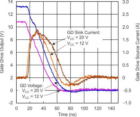
| Rise time | 1 V to 9 V, CLOAD = 1 nF | 18 | 30 | ns | ||
| Fall time | 9 V to 1 V, CLOAD = 1 nF | 12 | 25 | |||
| GDA, GDB output voltage, UVLO | VCC = 3.0 V, IGDA, IGDB = 2.5 mA | 100 | 200 | mV | ||
| ZERO CURRENT DETECTOR | ||||||
| ZCDA, ZCDB voltage threshold, falling | 0.8 | 1 | 1.2 | V | ||
| ZCDA, ZCDB voltage threshold, rising | 1.5 | 1.7 | 1.9 | |||
| ZCDA, ZCDB clamp, high | IZCDA = +2 mA, IZCDB = +2 mA | 2.6 | 3 | 3.4 | ||
| ZCDA, ZCDB clamp, low | IZCDA = −2 mA, IZCDB = −2 mA | 0 | −0.2 | −0.4 | ||
| ZCDA, ZCDB input bias current | ZCDA = 1.4 V, ZCDB = 1.4 V | ±0.03 | ±0.5 | µA | ||
| ZCDA, ZCDB delay to GDA, GDB outputs(2) | From ZCDx input falling to 1 V to respective gate drive output rising 10% | 50 | 100 | ns | ||
| ZCDA blanking time(3) | From GDA rising and GDA falling | 100 | ||||
| ZCDB blanking time(3) | From GDB rising and GDB falling | 100 | ||||
| CURRENT SENSE | ||||||
| CS input bias current, dual-phase | At rising threshold | −120 | −166 | −200 | µA | |
| CS current-limit rising threshold, dual-phase | PHB = 5 V | −0.18 | −0.2 | −0.22 | V | |
| CS current-limit rising threshold, single-phase | PHB = 0 V | −0.149 | −0.166 | −0.183 | ||
| CS current-limit reset falling threshold | −0.003 | –0.015 | −0.025 | |||
| CS current-limit response time(2) | From CS exceeding threshold−0.05 V to GDx dropping 10% | 60 | 100 | ns | ||
| CS blanking time | From GDx rising and falling edges | 100 | ||||
| VINAC INPUT | ||||||
| IVINAC | VINAC input bias current, above brownout | VINAC = 2 V | ±0.03 | ±0.5 | µA | |
| VBODET | VINAC brownout detection threshold | VINAC falling | 1.33 | 1.39 | 1.44 | V |
| tBODLY | VINAC brownout filter time | VINAC below the brownout detection threshold for the brownout filter time | 340 | 440 | 540 | ms |
| VBOHYS | VINAC brownout threshold hysteresis | VINAC rising | 30 | 62 | 75 | mV |
| IBOHYS | VINAC brownout hysteresis current | VINAC = 1 V for > tBODLY | 1.6 | 2 | 2.5 | µA |
| VDODET | VINAC dropout detection threshold | VINAC falling | 0.315 | 0.35 | 0.38 | V |
| tDODLY | VINAC dropout filter time | VINAC below the dropout detection threshold for the dropout filter time | 3.5 | 5 | 7 | ms |
| VDOCLR | VINAC dropout clear threshold | VINAC rising | 0.67 | 0.71 | 0.75 | V |
| PULSE-WIDTH MODULATOR | ||||||
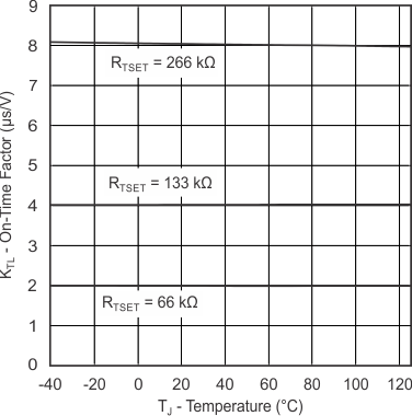
| KT | On-time factor, phases A and B | VSENSE = 5.8 V(4) | 3.6 | 4.0 | 4.4 | µs/V |
| KTS | On-time factor, single-phase, A | VSENSE = 5.8 V, PHB = 0 V(4) | 7.2 | 8.0 | 8.9 | |
| Phase B to phase A on-time matching error | VSENSE = 5.8 V | ±2% | ±6% | |||
| Zero-crossing distortion correction additional on time | COMP = 0.25 V, VINAC = 1 V | 1.2 | 2 | 2.8 | µs | |
| COMP = 0.25 V, VINAC = 0.1 V | 12.6 | 20 | 29 | |||
| VPHBF | PHB threshold falling, to single-phase operation | To GDB output shutdown, VINAC = 1.5 V | 0.7 | 0.8 | 0.9 | V |
| VPHBR | PHB threshold rising, to two-phase operation | To GDB output running, VINAC = 1.5 V | 0.9 | 1 | 1.1 | |
| TMIN | Minimum switching period | RTSET = 133 kΩ(4) | 1.7 | 2.2 | 3 | µs |
| TSTART | PWM restart time | ZCDA = ZCDB = 2 V(5) | 165 | 210 | 265 | |
| THERMAL SHUTDOWN | ||||||
| TJ | Thermal shutdown temperature | Temperature rising(6) | 160 | °C | ||
| TJ | Thermal restart temperature | Temperature falling(6) | 140 | |||
(1) Excessive VCC input voltage and current will damage the device. This clamp will not protect the device from an unregulated bias supply. If an unregulated bias supply is used, a series-connected Fixed Positive-Voltage Regulator such as the UA78L15A is recommended. See the Absolute Maximum Ratings table for the limits on VCC voltage, current, and junction temperature.
(2) Refer to Figure 13, Figure 14, Figure 15, and Figure 16 of the Typical Characteristics for typical gate drive waveforms.
(3) ZCD blanking times are ensured by design.
(4) Gate drive on-time is proportional to (VCOMP – 0.125 V). The on-time proportionality factor, KT, scales linearly with the value of RTSET and is different in two-phase and single-phase modes. The minimum switching period is proportional to RTSET.
(5) An output on-time is generated at both GDA and GDB if both ZCDA and ZCDB negative-going edges are not detected for the restart time. In single-phase mode, the restart time applies for the ZCDA input and the GDA output.
(6) Thermal shutdown occurs at temperatures higher than the normal operating range. Device performance above the normal operating temperature is not specified or assured.
7.6 Typical Characteristics
At VCC = 16 V, AGND = PGND = 0 V, VINAC = 3 V, VSENSE = 6 V, HVSEN = 3 V, PHB = 5 V, RTSET = 133 kΩ; all voltages are with respect to GND, all outputs unloaded, TJ = TA = +25 °C, and currents are positive into and negative out of the specified terminal, unless otherwise noted.


| IVREF = 0 to –2 mA |
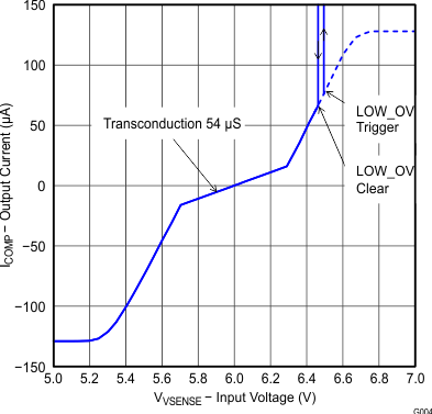
| Soft-Start Completed | ||

| 5.9 V < VVSENSE < 6.1 V | ||

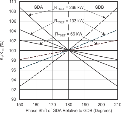
| KTO = 2(KTA × KTB) / KTA + KTB | ||

| CLOAD = 4.7 nF | ||

| CLOAD = 4.7 nF |
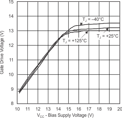
| RLOAD = 2.7 kΩ |

| Load = 100 mA |


| VCS = –195 mV |


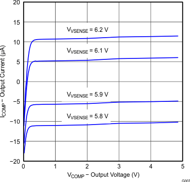

| CLOAD = 4.7 nF | ||

| CLOAD = 4.7 nF |

| RLOAD = 2.7 kΩ |


