SLUSC60B December 2017 – October 2019 UCC28064A
PRODUCTION DATA.
- 1 Features
- 2 Applications
- 3 Description
- 4 Revision History
- 5 Description (Continued)
- 6 Pin Configuration and Functions
- 7 Specifications
-
8 Detailed Description
- 8.1 Overview
- 8.2 Functional Block Diagram
- 8.3
Feature Description
- 8.3.1 Principles of Operation
- 8.3.2 Natural Interleaving
- 8.3.3 On-Time Control, Maximum Frequency Limiting, Restart Timer and Input Voltage Feed-Forward compensation
- 8.3.4 Distortion Reduction
- 8.3.5 Zero-Current Detection and Valley Switching
- 8.3.6 Phase Management and Light-Load Operation
- 8.3.7 Burst Mode Operation
- 8.3.8 External Disable
- 8.3.9 Improved Error Amplifier
- 8.3.10 Soft Start
- 8.3.11 Brownout Protection
- 8.3.12 Line Dropout Detection
- 8.3.13 VREF
- 8.3.14 VCC
- 8.3.15
System Level Protections
- 8.3.15.1 Failsafe OVP - Output Over-voltage Protection
- 8.3.15.2 Overcurrent Protection
- 8.3.15.3 Open-Loop Protection
- 8.3.15.4 VCC Undervoltage Lock-Out (UVLO) Protection
- 8.3.15.5 Phase-Fail Protection
- 8.3.15.6 CS - Open, TSET - Open and Short Protection
- 8.3.15.7 Thermal Shutdown Protection
- 8.3.15.8 Fault Logic Diagram
- 8.4 Device Functional Modes
-
9 Application and Implementation
- 9.1 Application Information
- 9.2
Typical Application
- 9.2.1 Design Requirements
- 9.2.2
Detailed Design Procedure
- 9.2.2.1 Custom Design With WEBENCH® Tools
- 9.2.2.2 Inductor Selection
- 9.2.2.3 ZCD Resistor Selection RZA, RZB
- 9.2.2.4 HVSEN
- 9.2.2.5 Output Capacitor Selection
- 9.2.2.6 Selecting RS For Peak Current Limiting
- 9.2.2.7 Power Semiconductor Selection (Q1, Q2, D1, D2)
- 9.2.2.8 Brownout Protection
- 9.2.2.9 Converter Timing
- 9.2.2.10 Programming VOUT
- 9.2.2.11 Voltage Loop Compensation
- 9.2.3 Application Curves
- 10Power Supply Recommendations
- 11Layout
- 12Package Option Addendum
- 13Device and Documentation Support
- 14Mechanical, Packaging, and Orderable Information
Package Options
Mechanical Data (Package|Pins)
- D|16
Thermal pad, mechanical data (Package|Pins)
Orderable Information
8.3.5 Zero-Current Detection and Valley Switching
In transition-mode PFC circuits, the MOSFET turns on when the boost inductor current reaches zero. Because of the resonance between the boost inductor and the parasitic capacitance at the MOSFET drain node, part of the energy stored in the MOSFET junction capacitor can be recovered, reducing switching losses. Furthermore, when the rectified input voltage is less than half of the output voltage, all the energy stored in the MOSFET junction capacitor can be recovered and zero-voltage switching (ZVS) can be realized. By adding an appropriate delay, the MOSFET can be turned on at the valley of its resonating drain voltage (valley-switching). In this way, the energy recovery can be maximized and switching loss is minimized.
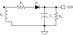
The optimal time delay is generally derived empirically, but a good starting point is a value equal to 25% of the resonant period of the drain circuit. The delay can be realized by a simple RC filter, as shown in Figure 18, but the delay time increases slightly as the input voltage nears the output voltage. Because the ZCD pin is internally clamped, a more accurate delay can also be realized by using the circuit shown in Figure 19.
 Figure 18. Simple RC Delay Circuit
  Figure 19. More Accurate Time Delay Circuit