SLUS577D November 2011 – August 2016 UCC2817A , UCC2818A , UCC3817A , UCC3818A
PRODUCTION DATA.
- 1 Features
- 2 Applications
- 3 Description
- 4 Revision
- 5 Description (Continued)
- 6 Device Comparison Tables
- 7 Pin Configuration and Functions
- 8 Specifications
- 9 Detailed Description
- 10Application and Implementation
- 11Power Supply Recommendations
- 12Layout
- 13Device and Documentation Support
- 14Mechanical, Packaging, and Orderable Information
Package Options
Refer to the PDF data sheet for device specific package drawings
Mechanical Data (Package|Pins)
- PW|16
- N|16
- D|16
Thermal pad, mechanical data (Package|Pins)
Orderable Information
9 Detailed Description
9.1 Overview
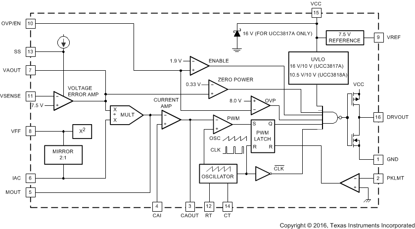
The UCC3817A and the UCC3818A family of products provides PFC controllers all the necessary functions for achieving near unity PFC.
The UCC3817A and UCC3818A, while being pin-compatible with other industry controllers providing similar functionality, offer many feature enhancements and tighter specifications, leading to an overall reduction in system implementation cost.
The system performance is enhanced by incorporating many innovative features such as average current-mode control which maintains stable noise immune low distortion sinusoidal current. Also, the IC features a leading edge modulation which when synchronized properly with a second stage DC-DC converter can reduce the ripple current on the output capacitor thereby increasing the overall lifetime of the power supply.
In addition to these features, the key difference between the UCC281xA and the UCC381xA is that the UCC2817A can work over the extended temperature range of –40 to 85°C as opposed to 0 to 70°C in the case of the UCC3817A.
9.2 Functional Block Diagram

9.3 Feature Description
9.3.1 Reference Section and Error Amplifier
The reference is a highly accurate 7-V reference with an accuracy of the reference is 1.5%.
The error amplifier is a classic voltage error amplifier and has a short circuit current capability of 20 mA.
9.3.2 Zero Power Block
When the output of the zero power comparator goes below 2.3 V, the zero power comparator latches the gate drive signal low.
9.3.3 Multiplier
The multiplier has 3 inputs. The inputs to the multiplier are VAOUT, the voltage amplifier error signal, IIAC, a representation of the input rectified AC line voltage, and an input voltage feedforward signal, VVFF.
The multiplier performs the calculation in Equation 1.
where
- K = 1/V
As the multiplier output is a current, this is a high-impedance input so the amplifier can be configured as a differential amplifier. This configuration improves noise immunity and allows for the leading-edge modulation operation.
9.3.4 Output Overvoltage Protection
When the output voltage exceeds the OVP threshold, the IC stops switching. The OVP reference is at 1.07%. There is also a 500 mV of hysteresis at the pin.
9.3.5 Pin Descriptions
9.3.5.1 CAI
Place a resistor between this pin and the GND side of current sense resistor. This input and the inverting input (MOUT) remain functional down to and below GND.
9.3.5.2 CAOUT
This is the output of a wide bandwidth operational amplifier that senses line current and commands the PFC pulse-width modulator (PWM) to force the correct duty cycle. Compensation components are placed between CAOUT and MOUT.
9.3.5.3 CT
A capacitor from CT to GND sets the PWM oscillator frequency according to Equation 2:

The lead from the oscillator timing capacitor to GND should be as short and direct as possible.
9.3.5.4 DRVOUT
The output drive for the boost switch is a totem-pole MOSFET gate driver on DRVOUT. To avoid the excessive overshoot of the DRVOUT while driving a capacitive load, a series gate current-limiting/damping resistor is recommended to prevent interaction between the gate impedance and the output driver. The value of the series gate resistor is based on the pulldown resistance (Rpulldown which is 4 Ω typical), the maximum VCC voltage (VCC), and the required maximum gate drive current (IMAX). Using Equation 3, a series gate resistance of resistance 11 Ω would be required for a maximum VCC voltage of 18 V and for 1.2 A of maximum sink current. The source current will be limited to approximately 900 mA (based on the Rpullup of 9-Ω typical).

9.3.5.5 GND
All voltages measured with respect to ground. VCC and REF should be bypassed directly to GND with a 0.1-µF or larger ceramic capacitor.
9.3.5.6 IAC
This input to the analog multiplier is a current proportional to instantaneous line voltage. The multiplier is tailored for very low distortion from this current input (IIAC) to multiplier output. The recommended maximum IIAC is
500 µA.
9.3.5.7 MOUT
The output of the analog multiplier and the inverting input of the current amplifier are connected together at MOUT. As the multiplier output is a current, this is a high-impedance input so the amplifier can be configured as a differential amplifier. This configuration improves noise immunity and allows for the leading-edge modulation operation. The multiplier output current is limited to (2 × IIAC). The multiplier output current is given by Equation 4:

where  is the multiplier gain constant.
9.3.5.8 OVP/EN
A window comparator input that disables the output driver if the boost output voltage is a programmed level above the nominal or disables both the PFC output driver and resets SS if pulled below 1.9 V (typical).
9.3.5.9 PKLMT
The threshold for peak limit is 0 V. Use a resistor divider from the negative side of the current sense resistor to VREF to level shift this signal to a voltage level defined by the value of the sense resistor and the peak current limit. Peak current limit is reached when PKLMT voltage falls below 0 V.
9.3.5.10 RT
A resistor from RT to GND is used to program oscillator charging current. TI recommends a resistor between
10 kΩ and 100 kΩ. Nominal voltage on this pin is 3 V.
9.3.5.11 SS
VSS is discharged for VVCC low conditions. When enabled, SS charges an external capacitor with a current source. This voltage is used as the voltage error signal during start-up, enabling the PWM duty cycle to increase slowly. In the event of a VVCC dropout, the OVP/EN is forced below 1.9 V (typ), SS quickly discharges to disable the PWM.
NOTE
In an open-loop test circuit, grounding the SS pin does not ensure 0% duty cycle. See the application section for details.
9.3.5.12 VAOUT
This is the output of the operational amplifier that regulates output voltage. The voltage amplifier output is internally limited to approximately 5.5 V to prevent overshoot.
9.3.5.13 VCC
Connect to a stable source of at least 20 mA from 10 V to 17 V for normal operation. Bypass VCC directly to GND to absorb supply current spikes required to charge external MOSFET gate capacitances. To prevent inadequate gate drive signals, the output devices are inhibited unless VVCC exceeds the upper undervoltage lockout voltage threshold and remains above the lower threshold.
9.3.5.14 VFF
The RMS voltage signal generated at this pin by mirroring 1/2 of the IIAC into a single pole external filter. At low line, the VFF voltage should be 1.4 V.
9.3.5.15 VSENSE
This is normally connected to a compensation network and to the boost converter output through a divider network.
9.3.5.16 VREF
VREF is the output of an accurate 7.5-V voltage reference. This output is capable of delivering 20 mA to peripheral circuitry and is internally short-circuit current limited. VREF is disabled and remains at 0 V when VVCC is below the UVLO threshold. Bypass VREF to GND with a 0.1-µF or larger ceramic capacitor for best stability. See Figure 12 and Figure 13 for VREF line and load regulation characteristics.
9.4 Device Functional Modes
9.4.1 Transition Mode Control
The boost converter, the most common topology used for power factor correction, can operate in two modes: continuous conduction code (CCM) and discontinuous conduction mode (DCM). Transition mode control, also referred to as critical conduction mode (CRM) or boundary conduction mode, maintains the converter at the boundary between CCM and DCM by adjusting the switching frequency.
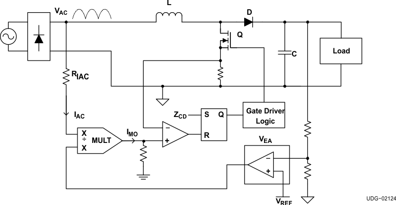
The CRM converter typically uses a variation of hysteretic control, with the lower boundary equal to zero current. It is a variable frequency control technique that has inherently stable input current control while eliminating reverse recovery rectifier losses. As shown in Figure 3, the switch current is compared to the reference signal (output of the multiplier) directly. This control method has the advantage of simple implementation and good power factor correction.
 Figure 3. Basic Block Diagram of CRM Boost PFC
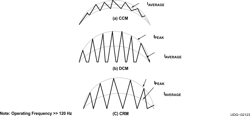
The power stage equations and the transfer functions of the CRM are the same as the CCM. However, implementations of the control functions are different. Transition mode forces the inductor current to operate just at the border of CCM and DCM. The current profile is also different, and affects the component power loss and filtering requirements. The peak current in the CRM boost is twice the amplitude of CCM, leading to higher conduction losses. The peak-to-peak ripple is twice the average current, which affects MOSFET switching losses and magnetics ac losses.
 Figure 4. PFC Inductor Current Profiles
For low to medium power applications up to approximately 300 W, the CRM boost has an advantage in losses. The filtering requirement is not severe, and therefore is not a disadvantage. For medium to higher power applications, where the input filter requirements dominate the size of the magnetics, the CCM boost is a good choice due to lower peak currents (which reduces conduction losses) and lower ripple current (which reduces filter requirements). The main tradeoff in using CRM boost is lower losses due to no reverse recovery in the boost diode vs higher ripple and peak currents.