SLUS646K November 2005 – August 2015 UCC28600
PRODUCTION DATA.
- 1 Features
- 2 Applications
- 3 Description
- 4 Revision History
- 5 Pin Configuration and Functions
- 6 Specifications
- 7 Detailed Description
- 8 Application and Implementation
- 9 Power Supply Recommendations
- 10Layout
- 11Device and Documentation Support
- 12Mechanical, Packaging, and Orderable Information
Package Options
Refer to the PDF data sheet for device specific package drawings
Mechanical Data (Package|Pins)
- D|8
Thermal pad, mechanical data (Package|Pins)
Orderable Information
1 Features
- Green-Mode Controller With Advanced Energy Saving Features
- Quasi-Resonant Mode Operation for Reduced EMI and Low Switching Losses (Low-Voltage Valley Switching)
- Low Standby Current for Minimum System No-Load Power Consumption
- Low Start-up Current: 25-μA Maximum
- Programmable Line and Load Over-Voltage Protection
- Internal Over-Temperature Protection
- Current Limit Protection
- Cycle-by-Cycle Power Limit
- Primary-Side Over-Current Hiccup Restart Mode
- 1-A Sink, –0.75-A Source TrueDrive™ Gate Drive Output
- Programmable Soft-Start
- Green-Mode Status Pin (PFC Disable Function)
2 Applications
3 Description
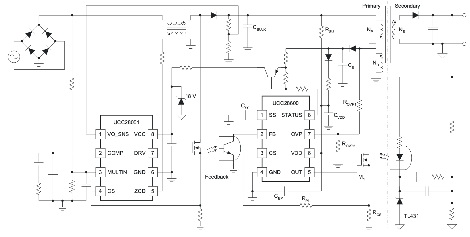
The UCC28600 is a PWM controller with advanced energy features to meet stringent world-wide energy efficiency requirements.
UCC28600 integrates built-in advanced energy saving features with high-level protection features to provide cost-effective solutions for energy-efficient power supplies. UCC28600 incorporates frequency fold-back and green-mode operation to reduce the switching losses at light-load and no-load conditions.
UCC28600 is available in the 8-pin SOIC package. Operating junction temperature range is –40°C to +105°C.
The UCC28600 Design Calculator, (SLVC104), located in the Tools and Software section of the UCC28600 product folder, provides a user-interactive iterative process for selecting recommended component values for an optimal design.
Device Information (1)
| PART NUMBER | PACKAGE | BODY SIZE (NOM) |
|---|---|---|
| UCC28600 | SOIC (8) | 4.90 mm × 3.91 mm |
- For all available packages, see the orderable addendum at the end of the data sheet.
Typical Application Diagram
