SLUSD12A October 2017 – February 2018 UCC28780
PRODUCTION DATA.
- 1 Features
- 2 Applications
- 3 Description
- 4 Revision History
- 5 Pin Configuration and Functions
- 6 Specifications
-
7 Detailed Description
- 7.1 Overview
- 7.2 Functional Block Diagram
- 7.3
Detailed Pin Description
- 7.3.1 BUR Pin (Programmable Burst Mode)
- 7.3.2 FB Pin (Feedback Pin)
- 7.3.3 VDD Pin (Device Bias Supply)
- 7.3.4 REF Pin (Internal 5-V Bias)
- 7.3.5 HVG and SWS Pins
- 7.3.6 RTZ Pin (Sets Delay for Transition Time to Zero)
- 7.3.7 RDM Pin (Sets Synthesized Demagnetization Time for ZVS Tuning)
- 7.3.8 RUN Pin (Driver Enable Pin)
- 7.3.9 SET Pin
- 7.4
Device Functional Modes
- 7.4.1 Adaptive ZVS Control with Auto-Tuning
- 7.4.2 Dead-Time Optimization
- 7.4.3 Control Law across Entire Load Range
- 7.4.4 Adaptive Amplitude Modulation (AAM)
- 7.4.5 Adaptive Burst Mode (ABM)
- 7.4.6 Low Power Mode (LPM)
- 7.4.7 Standby Power Mode (SBP)
- 7.4.8 Startup Sequence
- 7.4.9 Survival Mode of VDD
- 7.4.10 System Fault Protections
- 7.4.11 Pin Open/Short Protections
-
8 Application and Implementation
- 8.1 Application Information
- 8.2
Typical Application Circuit
- 8.2.1 Design Requirements
- 8.2.2 Detailed Design Procedure
- 8.2.3 Application Curves
- 9 Power Supply Recommendations
- 10Layout
- 11Device and Documentation Support
- 12Mechanical, Packaging, and Orderable Information
Package Options
Refer to the PDF data sheet for device specific package drawings
Mechanical Data (Package|Pins)
- D|16
- RTE|16
Thermal pad, mechanical data (Package|Pins)
- RTE|16
Orderable Information
7.4.8 Startup Sequence
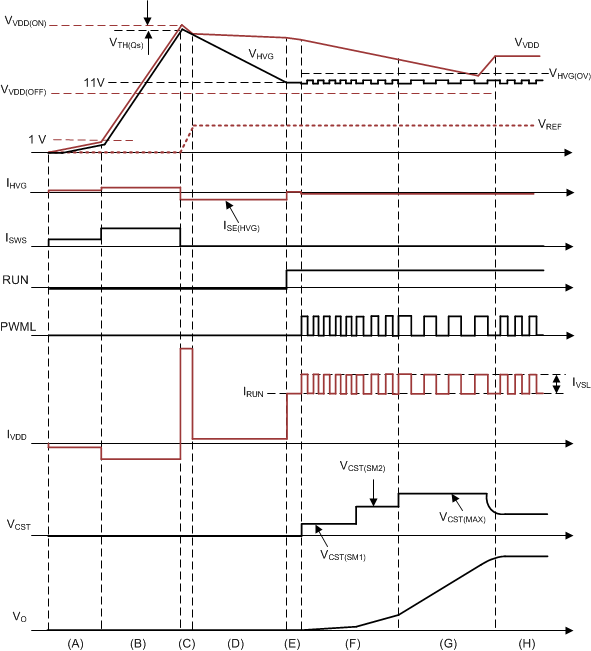
Figure 29 shows the simplified block diagram related with the VDD startup function of UCC28780, and Figure 30 addresses the startup sequence. The detailed description on the startup waveforms is :
- Time interval A: The UVLO circuit commands the two internal power-path switches (QDDS and QDDH) to build connections among SWS, VDD, and HVG pins through two serial current-limiting resistors (RDDS and RDDH). The depletion-mode MOSFET (QS) starts sourcing charge current (ISWS) safely from the high-voltage switch-node voltage (VSW) to the VDD capacitor (CVDD). Before VVDD reaches 1 V, ISWS is limited by the high-resistance RDDS of 12 kΩ to prevent potential device damage if CVDD or VDD pin is shorted to ground.
- Time interval B: After VVDD rises above 1 V, RDDS is reduced to a smaller resistance of 1 kΩ. ISWS is increased to charge CVDD faster. The maximum charge current during VDD startup can be quantified by Equation 7.
- Time interval C: As VVDD reaches VVDD(ON) of 17.5 V, the ULVO circuit turns-off QDDS to disconnect the source pin of QS to CVDD, and turns-off QDDH to break the gate-to-source connection of QS, so QS loses its current-charge capability. VDD then starts to drop, because the 5-V regulator on REF pin starts to charge up the reference capacitor (CREF) to 5 V, which maximum charge current (ISE(REF)) is self-limited at around 14 mA. After VREF is settled, the UVLO circuit turns-on another power-path switch (Q11H), so an internal 11-V regulator is connected to the HVG pin. The voltage on the HVG pin capacitor (CHVG) starts to be discharged by the regulator.
- Time interval D: During discharging CHVG of the recommended 2.2 nF, the sink current of the 11-V regulator (ISE(HVG)) is self-limited at around 90 μA, so it takes longer than 25 μs for settling to 11 V. If VHVG reaches 11 V in less than 10 to 25 μs, the HVG pin open fault is triggered to protect the device. Once VHVG is settled to 11 V without the fault event, RUN pin goes high and UCC28780 enters a run state with IVDD = IRUN.
- Time interval E: There is a 2.2-μs delay from RUN going high to PWML starting to switch in order to wake-up the gate driver and UCC28780.
- Time interval F: This is the soft-start region of peak magnetizing current. The first purpose is to limit the supply current if the output is short. The second purpose is to push the switching frequency higher than the audible frequency range during repetitive startup situations. At the beginning of VO soft-start, the peak current is limited by two VCST thresholds. The first VCST startup threshold (VCST(SM1)) is clamped at 0.28 V and the following second threshold (VCST(SM2)) is 0.6 V. When VCST = VCST(SM1), PWMH is disabled if the VS pin voltage (VVS) < 0.28 V, and the first five PWML pulses are forced to stay at this current level. After VVS exceeds 0.28 V and the first five PWML pulses are generated, the peak current threshold changes from VCST(SM1) to VCST(SM2). In case of the inability to build up VO with VCST(SM1) at the beginning of the VO soft-start due to excessively large output capacitor and/or constant-current output load, there is an internal time-out of 1ms to force VCST to switch to VCST(SM2).
- Time interval G: When VVS rises above 0.6 V, VCST is allowed to reach VCST(MAX) of 0.8 V, so the rising rate of VO startup becomes faster. When PWML is in a high state, IVDD can be larger than IRUN, because the 5-V regulator provides the line-sensing current pulse (IVSL) on the VS pin to sense VBULK condition.
- Time interval H: VO and VCST settle, and the auxiliary winding takes over the VDD supply. There is a switching ripple on CHVG during PWML switching, due to the dV/dt coupling of VSW through the junction capacitance of QS. UCC28780 provides an over-voltage protection on HVG pin to avoid the risk of high overshoot under high dV/dt conditions. The over-voltage threshold of HVG pin (VHVG(OV)) is 13.8V.
 Figure 29. Functional Startup Block Diagram
 Figure 30. Startup Timing Waveforms