SLUSDB2B August 2018 – October 2024 UCC28950 , UCC28951
PRODUCTION DATA
- 1
- 1 Features
- 2 Applications
- 3 Description
- 4 Pin Configuration and Functions
- 5 Specifications
-
6 Detailed Description
- 6.1 Overview
- 6.2 Functional Block Diagram
- 6.3
Feature Description
- 6.3.1 Start-Up Protection Logic
- 6.3.2 Voltage Reference (VREF)
- 6.3.3 Error Amplifier (EA+, EA–, COMP)
- 6.3.4 Soft-Start and Enable (SS/EN)
- 6.3.5 Light-Load Power Saving Features
- 6.3.6 Adaptive Delay, (Delay Between OUTA and OUTB, OUTC and OUTD (DELAB, DELCD, ADEL))
- 6.3.7 Adaptive Delay (Delay Between OUTA and OUTF, OUTB and OUTE (DELEF, ADELEF)
- 6.3.8 Minimum Pulse (TMIN)
- 6.3.9 Burst Mode
- 6.3.10 Switching Frequency Setting
- 6.3.11 Slope Compensation (RSUM)
- 6.3.12 Dynamic SR ON/OFF Control (DCM Mode)
- 6.3.13 Current Sensing (CS)
- 6.3.14 Cycle-by-Cycle Current Limit Current Protection and Hiccup Mode
- 6.3.15 Synchronization (SYNC)
- 6.3.16 Outputs (OUTA, OUTB, OUTC, OUTD, OUTE, OUTF)
- 6.3.17 Supply Voltage (VDD)
- 6.3.18 Ground (GND)
- 6.4 Device Functional Modes
-
7 Application and Implementation
- 7.1 Application Information
- 7.2
Typical Application
- 7.2.1 Design Requirements
- 7.2.2
Detailed Design Procedure
- 7.2.2.1 Power Loss Budget
- 7.2.2.2 Preliminary Transformer Calculations (T1)
- 7.2.2.3 QA, QB, QC, QD FET Selection
- 7.2.2.4 Selecting LS
- 7.2.2.5 Selecting Diodes DB and DC
- 7.2.2.6 Output Inductor Selection (LOUT)
- 7.2.2.7 Output Capacitance (COUT)
- 7.2.2.8 Select FETs QE and QF
- 7.2.2.9 Input Capacitance (CIN)
- 7.2.2.10 Current Sense Network (CT, RCS, R7, DA)
- 7.2.3 Application Curves
- 7.3 Power Supply Recommendations
- 7.4 Layout
- 8 Device and Documentation Support
- 9 Revision History
- 10Mechanical, Packaging, and Orderable Information
Package Options
Mechanical Data (Package|Pins)
- PW|24
Thermal pad, mechanical data (Package|Pins)
Orderable Information
7.2.2.8 Select FETs QE and QF
Selecting FETs for a design is an iterative process. To meet the power requirements of this design, we select 75V, 120A FETs, from Fairchild, part number FDP032N08. These FETs have the following characteristics.
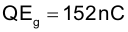
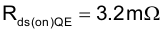
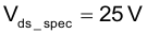
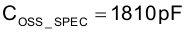
Calculate average FET COSS (COSS_QE_AVG) based on the data sheet parameters for COSS (COSS_SPEC), and drain to source voltage where COSS_SPEC was measured (Vds_spec), and the maximum drain to source voltage in the design (VdsQE) that will be applied to the FET in the application.
The voltage across FET QE and QF when they are of isf:

The voltage where FET COSS is specified and tested in the FET data sheet:
The specified output capacitance from FET data sheet is:
The average QE and QF COSS [2] is calculated using Equation 80:

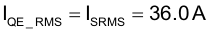
The QE and QF RMS current are:
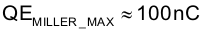
To estimate FET switching loss the Vg vs. Qg curve from the FET data sheet needs to be studied. First the gate charge at the beginning of the miller plateau needs to be determined (QEMILLER_MIN) and the gate charge at the end of the miller plateau (QEMILLER_MAX) for the given VDS.
The maximum gate charge at the end of the miller plateau is:
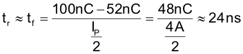
The minimum gate charge at the beginning of the miller plateau is:

The FETs in this design are driven with a UCC27324 Gate Driver IC, setup to drive 4A (IP) of gate drive current.

Estimated FET Vds rise and fall time using Equation 85:
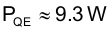
Estimate QE and QF FET Losses (PQE) using Equation 86:

Recalculate the power budget using Equation 88.
