SLUSDB2B August 2018 – October 2024 UCC28950 , UCC28951
PRODUCTION DATA
- 1
- 1 Features
- 2 Applications
- 3 Description
- 4 Pin Configuration and Functions
- 5 Specifications
-
6 Detailed Description
- 6.1 Overview
- 6.2 Functional Block Diagram
- 6.3
Feature Description
- 6.3.1 Start-Up Protection Logic
- 6.3.2 Voltage Reference (VREF)
- 6.3.3 Error Amplifier (EA+, EA–, COMP)
- 6.3.4 Soft-Start and Enable (SS/EN)
- 6.3.5 Light-Load Power Saving Features
- 6.3.6 Adaptive Delay, (Delay Between OUTA and OUTB, OUTC and OUTD (DELAB, DELCD, ADEL))
- 6.3.7 Adaptive Delay (Delay Between OUTA and OUTF, OUTB and OUTE (DELEF, ADELEF)
- 6.3.8 Minimum Pulse (TMIN)
- 6.3.9 Burst Mode
- 6.3.10 Switching Frequency Setting
- 6.3.11 Slope Compensation (RSUM)
- 6.3.12 Dynamic SR ON/OFF Control (DCM Mode)
- 6.3.13 Current Sensing (CS)
- 6.3.14 Cycle-by-Cycle Current Limit Current Protection and Hiccup Mode
- 6.3.15 Synchronization (SYNC)
- 6.3.16 Outputs (OUTA, OUTB, OUTC, OUTD, OUTE, OUTF)
- 6.3.17 Supply Voltage (VDD)
- 6.3.18 Ground (GND)
- 6.4 Device Functional Modes
-
7 Application and Implementation
- 7.1 Application Information
- 7.2
Typical Application
- 7.2.1 Design Requirements
- 7.2.2
Detailed Design Procedure
- 7.2.2.1 Power Loss Budget
- 7.2.2.2 Preliminary Transformer Calculations (T1)
- 7.2.2.3 QA, QB, QC, QD FET Selection
- 7.2.2.4 Selecting LS
- 7.2.2.5 Selecting Diodes DB and DC
- 7.2.2.6 Output Inductor Selection (LOUT)
- 7.2.2.7 Output Capacitance (COUT)
- 7.2.2.8 Select FETs QE and QF
- 7.2.2.9 Input Capacitance (CIN)
- 7.2.2.10 Current Sense Network (CT, RCS, R7, DA)
- 7.2.3 Application Curves
- 7.3 Power Supply Recommendations
- 7.4 Layout
- 8 Device and Documentation Support
- 9 Revision History
- 10Mechanical, Packaging, and Orderable Information
Package Options
Mechanical Data (Package|Pins)
- PW|24
Thermal pad, mechanical data (Package|Pins)
Orderable Information
7.2.2.9 Input Capacitance (CIN)
The input voltage in this design is 390VDC, which is typically fed by the output of a PFC boost pre-regulator. It is typical to select input capacitance based on holdup and ripple requirements.
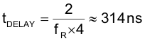
The delay time needed to achieve ZVS can act as a duty cycle clamp (DCLAMP).
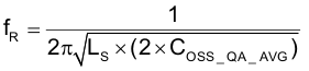
Calculate tank frequency using Equation 89:
Estimate the delay time using Equation 90:
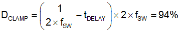
The effective duty cycle clamp (DCLAMP) is calculated in Equation 91:
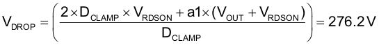
VDROP is the minimum input voltage where the converter can still maintain output regulation (see Equation 92). The converter’s input voltage would only drop down this low during a brownout or line-drop condition if this converter was following a PFC pre-regulator.
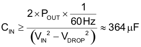
CIN was calculated in Equation 93 based on one line cycle of holdup:
Calculate the high-frequency input capacitor RMS current (ICINRMS) using Equation 94.
To meet the input capacitance and RMS current requirements for this design, a 330µF capacitor was chosen from Panasonic part number EETHC2W331EA:
CIN = 330µF
This capacitor has a high frequency (ESRCIN) of 150mΩ and is measured with an impedance analyzer at 200kHz. ESRCIN = 0.150Ω
Estimate the CIN power dissipation (PCIN) using Equation 95:

And recalculate the remaining power budget using Equation 96:

There is approximately 6.0W that remains in the power budget for the current-sensing network, to bias the control device, and for all resistors supporting the control device.