SLUS168E Apr 1999 – August 2015 UCC2808-1 , UCC2808-2 , UCC3808-1 , UCC3808-2
PRODUCTION DATA.
- 1 Features
- 2 Applications
- 3 Description
- 4 Revision History
- 5 Pin Configuration and Functions
- 6 Specifications
- 7 Detailed Description
- 8 Application and Implementation
- 9 Power Supply Recommendations
- 10Layout
- 11Device and Documentation Support
- 12Mechanical, Packaging, and Orderable Information
Package Options
Mechanical Data (Package|Pins)
- D|8
Thermal pad, mechanical data (Package|Pins)
Orderable Information
10 Layout
10.1 Layout Guidelines
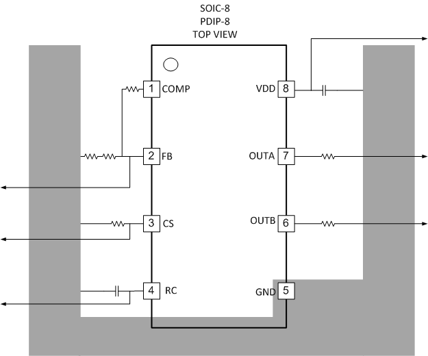
- Locate the VDD capacitor as close as possible between the VDD terminal and GND of the UCCx808-x, tracked directly to both terminals.
- A small, external filter capacitor is recommended on the CS terminal. Track the filter capacitor as directly as possible from the CS to GND terminal.
- The tracking and layout of the FB terminal and connecting components is critical to minimizing noise pick-up and interference in the magnetic sensing block. Reduce the total surface area of trances on the FB net to a minimum.
- The OUTA/OUTB terminal has high internal sink/source current capability. An external gate resistor is recommended. The value depends on the choice of power MOSFET, efficiency and EMI considerations. A pulldown resistor on the gate of the external MOSFET is recommended to prevent the MOSFET gate from floating on if there is an open-circuit error in the gate drive path.
10.2 Layout Example
 Figure 9. Layout Example