SLUS577D November 2011 – August 2016 UCC2817A , UCC2818A , UCC3817A , UCC3818A
PRODUCTION DATA.
- 1 Features
- 2 Applications
- 3 Description
- 4 Revision
- 5 Description (Continued)
- 6 Device Comparison Tables
- 7 Pin Configuration and Functions
- 8 Specifications
- 9 Detailed Description
- 10Application and Implementation
- 11Power Supply Recommendations
- 12Layout
- 13Device and Documentation Support
- 14Mechanical, Packaging, and Orderable Information
Package Options
Refer to the PDF data sheet for device specific package drawings
Mechanical Data (Package|Pins)
- N|16
- D|16
Thermal pad, mechanical data (Package|Pins)
Orderable Information
8 Specifications
8.1 Absolute Maximum Ratings
over operating free-air temperature range (unless otherwise noted)(1)| MIN | MAX | UNIT | |
|---|---|---|---|
| Supply voltage VCC | 18 | V | |
| Supply current ICC | 20 | mA | |
| Gate drive current, continuous | 0.2 | A | |
| Gate drive current | 1.2 | A | |
| Input voltage, CAI, MOUT, SS | 8 | V | |
| Input voltage, PKLMT | 5 | V | |
| Input voltage, VSENSE, OVP/EN | 10 | V | |
| Input current, RT, IAC, PKLMT | 10 | mA | |
| Input current, VCC (no switching) | 20 | mA | |
| Maximum negative voltage, DRVOUT, PKLMT, MOUT | –0.5 | V | |
| Power dissipation | 1 | W | |
| Lead temperature, Tsol (soldering, 10 seconds) | 300 | °C | |
| Power dissipation | 1 | W | |
| Junction temperature, TJ | –55 | 150 | °C |
| Storage temperature, Tstg | –65 | 150 | °C |
(1) Stresses beyond those listed under Absolute Maximum Ratings may cause permanent damage to the device. These are stress ratings only, which do not imply functional operation of the device at these or any other conditions beyond those indicated under Recommended Operating Conditions. Exposure to absolute-maximum-rated conditions for extended periods may affect device reliability.
8.2 ESD Ratings
| VALUE | UNIT | |||
|---|---|---|---|---|
| V(ESD) | Electrostatic discharge | Human-body model (HBM), per ANSI/ESDA/JEDEC JS-001(1) | ±2000 | V |
| Charged-device model (CDM), per JEDEC specification JESD22-C101(2) | ±1500 | |||
(1) JEDEC document JEP155 states that 500-V HBM allows safe manufacturing with a standard ESD control process.
(2) JEDEC document JEP157 states that 250-V CDM allows safe manufacturing with a standard ESD control process.
8.3 Recommended Operating Conditions
over operating free-air temperature range (unless otherwise noted)| MIN | NOM | MAX | UNIT | ||
|---|---|---|---|---|---|
| VCC | Input voltage | 12 | 18 | V | |
| VSENSE | Input sense voltage | 7.5 | 10 | V | |
| Input current for oscillator | 1.36 | 10 | mA | ||
8.4 Thermal Information
| THERMAL METRIC(1) | UCCx81xA | UNIT | |||
|---|---|---|---|---|---|
| D (SOIC) | N (PDIP) | PW (TSSOP) | |||
| 16 PINS | 16 PINS | 16 PINS | |||
| RθJA | Junction-to-ambient thermal resistance | 73.9 | 49.3 | 98.9 | °C/W |
| RθJC(top) | Junction-to-case (top) thermal resistance | 33.5 | 38.9 | 30.2 | °C/W |
| RθJB | Junction-to-board thermal resistance | 31.4 | 29.4 | 44.8 | °C/W |
| ψJT | Junction-to-top characterization parameter | 5.8 | 18.9 | 1.9 | °C/W |
| ψJB | Junction-to-board characterization parameter | 31.1 | 29.2 | 44.1 | °C/W |
(1) For more information about traditional and new thermal metrics, see the Semiconductor and IC Package Thermal Metrics application report.
8.5 Electrical Characteristics
TA = 0°C to 70°C for the UCC3817A and TA = –40°C to 85°C for the UCC2817A, TA = TJ, VCC = 12 V, RT = 22 kΩ, CT = 270 pF, (unless otherwise noted)| PARAMETER | TEST CONDITIONS | MIN | TYP | MAX | UNIT |
|---|---|---|---|---|---|
| SUPPLY CURRENT SECTION | |||||
| Supply current, OFF | VCC = (VCC turnon threshold –0.3 V) | 150 | 300 | µA | |
| Supply current, ON | VCC = 12 V, No load on DRVOUT | 2 | 4 | 6 | mA |
| UVLO SECTION | |||||
| VCC turnon threshold (UCCx817) | 15.4 | 16 | 16.6 | V | |
| VCC turnoff threshold (UCCx817) | 9.4 | 9.7 | V | ||
| UVLO hysteresis (UCCx817) | 5.8 | 6.3 | V | ||
| Maximum shunt voltage (UCCx817) | IVCC = 10 mA | 15.4 | 17 | 17.5 | V |
| VCC turnon threshold (UCCx818) | 9.7 | 10.2 | 10.8 | V | |
| VCC turnoff threshold (UCCx818) | 9.4 | 9.7 | V | ||
| UVLO hysteresis (UCCx818) | 0.3 | 0.5 | V | ||
| VOLTAGE AMPLIFIER SECTION | |||||
| Input voltage | TA = 0°C to 70°C | 7.387 | 7.5 | 7.613 | V |
| TA = -–40°C to 85°C | 7.369 | 7.5 | 7.631 | ||
| VSENSE bias current | VSENSE = VREF, VAOUT = 2.5 V | 50 | 200 | nA | |
| Open-loop gain | VAOUT = 2 V to 5 V | 50 | 90 | dB | |
| High-level output voltage | IL = –150 µA | 5.3 | 5.5 | 5.6 | V |
| Low-level output voltage | IL = 150 µA | 0 | 50 | 150 | mV |
| OVER VOLTAGE PROTECTION AND ENABLE SECTION | |||||
| Over voltage reference | VREF +0.48 | VREF +0.50 | VREF +0.52 | V | |
| Hysteresis | 300 | 500 | 600 | mV | |
| Enable threshold | 1.7 | 1.9 | 2.1 | V | |
| Enable hysteresis | 0.1 | 0. | 0.3 | V | |
| CURRENT AMPLIFIER SECTION | |||||
| Input offset voltage | VCM = 0 V, VCAOUT = 3 V | –3.5 | 0 | 2.5 | mV |
| Input bias current | VCM = 0 V, VCAOUT = 3 V | –50 | –100 | nA | |
| Input offset current | VCM = 0 V, VCAOUT = 3 V | 25 | 100 | nA | |
| Open loop gain | VCM = 0 V, VCAOUT = 2 V to 5 V | 90 | dB | ||
| Common-mode output voltage | VCM = 0 V to 1.5 V, VCAOUT = 3 V | 60 | 80 | dB | |
| High-level output voltage | IL = –120 mA | 5.6 | 6.5 | 6.8 | VV |
| Low-level output voltage | IL = 1 mA | 0.1 | 0.2 | 0.5 | MHz |
| Gain bandwidth product | See (1) | 2.5 | |||
| VOLTAGE REFERENCE SECTION | |||||
| Input voltage | TA = 0°C to 70°C | 7.387 | 7.5 | 7.613 | V |
| TA = -–40°C to 85°C | 7.369 | 7.5 | 7.631 | ||
| Load regulation | IREF = 1 mA to 2 mA | 0 | 10 | mV | |
| Line regulation | VCC = 10.8 to 15 V(2) | 0 | 10 | mV | |
| Short-circuit current | VREF = 0 V | –20 | –25 | –50 | mA |
| OSCILLATOR SECTION | |||||
| Initial accuracy | TA = 25°C | 85 | 100 | 115 | kHz |
| Voltage stability | VCC = 10.8 to 15 V | –1% | 1% | ||
| Total variation | Line, temp | 80 | 120 | kHz | |
| Ramp peak voltage | 4.5 | 5 | 5.5 | V | |
| Ramp amplitude voltage (peak to peak) | 3.5 | 4 | 4.5 | V | |
| PEAK CURRENT LIMIT SECTION | |||||
| PKLMT reference voltage | –15 | 15 | mV | ||
| PKLMT propagation delay | 150 | 350 | 500 | ns | |
| MULTIPLIER SECTION | |||||
| IMOUT, high line, low power output current, (0°C to 85°C) | IAC = 500 µA, VFF = 4.7 V, VAOUT = 1.25 V | 0 | –6 | –20 | µA |
| IMOUT, high line, low power output current, (–40°C to 85°C) | IAC = 500 µA, VFF = 4.7 V, VAOUT = 1.25 V | 0 | –6 | –23 | |
| IMOUT, high line, low power output current | IAC = 500 µA, VFF = 4.7 V, VAOUT = 5 V | –70 | –90 | –105 | |
| IMOUT, low line, low power output current | IAC = 150 µA, VFF = 1.4 V, VAOUT = 1.25 V | –10 | –19 | –50 | |
| IMOUT, low line, high power output current | IAC = 150 µA, VFF = 1.4 V, VAOUT = 5 V | –268 | –300 | –345 | |
| IMOUT, IAC limited output current | IAC = 150 µA, VFF = 1.3 V, VAOUT = 5 V | –250 | –300 | –400 | |
| Gain constant (K) | IAC = 150 µA, VFF = 1.3 V, VAOUT = 2.5 V | 0.5 | 1 | 1.5 | 1/V |
| IMOUT, zero current | IAC = 150 µA, VFF = 1.4 V, VAOUT = 0.25 V | 0 | –2 | µA | |
| IAC = 500 µA, VFF = 4.7 V, VAOUT = 0.25 V | 0 | –2 | |||
| IMOUT, zero current, (0°C to 85°C) | IAC = 500 µA, VFF = 4.7 V, VAOUT = 0.5 V | 0 | –3 | µA | |
| IMOUT, zero current, (–40°C to 85°C) | IAC = 500 µA, VFF = 4.7 V, VAOUT = 0.5 V | 0 | –3.5 | ||
| Power limit (IMOUT x VFF) | IAC = 150 µA, VFF = 1.4 V, VAOUT = 5 V | –375 | –420 | –485 | µW |
| FEED-FORWARD SECTION | |||||
| VFF output current | IAC = 300 µA | –140 | –150 | –160 | µA |
| SOFT START SECTION | |||||
| SS charge current | –6 | –10 | –16 | µA | |
| GATE DRIVER SECTION | |||||
| Pullup resistance | IO = –100 mA to –200 mA | 9 | 12 | Ω | |
| Pulldown resistance | IO = 100 mA | 4 | 10 | ||
| Output rise time | CL = 1 nF, RL = 10 Ω, VDRVOUT = 0.7 V to 9 V | 25 | 50 | ns | |
| Output fall time | CL = 1 nF, RL = 10 Ω, VDRVOUT = 9 V to 0.7 V | 10 | 50 | ||
| Maximum duty cycle | 93% | 95% | 99% | ||
| Minimum controlled duty cycle | At 100 kHz | 2% | |||
| ZERO POWER SECTION | |||||
| Zero power comparator threshold | Measured on VAOUT | 0.2 | 0.33 | 0.5 | V |
(1) Ensured by design, not production tested.
(2) Reference variation for VCC < 10.8 V is shown in Figure 12.
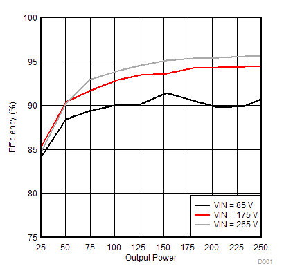
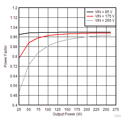
8.6 Typical Characteristics

