SLUS577D November 2011 – August 2016 UCC2817A , UCC2818A , UCC3817A , UCC3818A
PRODUCTION DATA.
- 1 Features
- 2 Applications
- 3 Description
- 4 Revision
- 5 Description (Continued)
- 6 Device Comparison Tables
- 7 Pin Configuration and Functions
- 8 Specifications
- 9 Detailed Description
- 10Application and Implementation
- 11Power Supply Recommendations
- 12Layout
- 13Device and Documentation Support
- 14Mechanical, Packaging, and Orderable Information
Package Options
Refer to the PDF data sheet for device specific package drawings
Mechanical Data (Package|Pins)
- PW|16
- N|16
- D|16
Thermal pad, mechanical data (Package|Pins)
Orderable Information
1 Features
- Controls Boost Preregulator to Near-Unity Power Factor
- Limits Line Distortion
- World Wide Line Operation
- Overvoltage Protection
- Accurate Power Limiting
- Average Current Mode Control
- Improved Noise Immunity
- Improved Feed-Forward Line Regulation
- Leading Edge Modulation
- 150-µA Typical Start-Up Current
- Low-Power BiCMOS Operation
- 12-V to 17-V Operation
- Frequency Range of 6 kHz to 220 kHz
2 Applications
- PC Power
- Consumer Electronics
- Lighting
- Industrial Power Supplies
- IEC6100-3-2 Compliant Supplies Less Than
300 W
3 Description
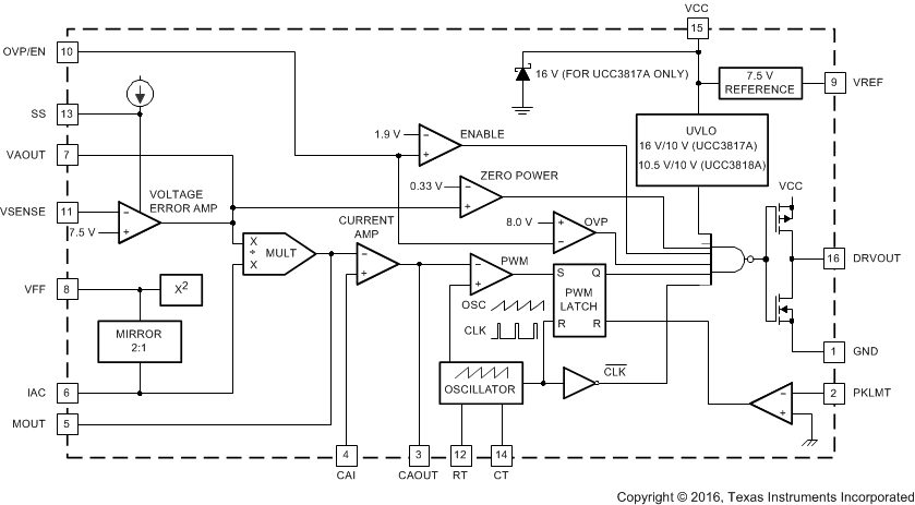
The UCC3817A and the UCC3818A family provides all the functions necessary for active power factor corrected preregulators. The controller achieves near unity power factor by shaping the ac input line current waveform to correspond to that of the ac input line voltage. Average current mode control maintains stable, low distortion sinusoidal line current.
Designed in Texas Instrument's BiCMOS process, the UCC3817A/UCC3818A offers new features such as lower start-up current, lower power dissipation, overvoltage protection, a shunt UVLO detect circuitry, a leading-edge modulation technique to reduce ripple current in the bulk capacitor and an improved, low-offset (±2 mV) current amplifier to reduce distortion at light load conditions.
Device Information(1)
| PART NUMBER | PACKAGE | BODY SIZE (NOM) |
|---|---|---|
| UCCx81xA | SOIC (16) | 4.90 mm × 3.91 mm |
| PDIP (16) | 19.30 mm × 6.35 mm | |
| TSSOP (16) | 5.00 mm × 4.40 mm |
- For all available packages, see the orderable addendum at the end of the data sheet.
Block Diagram
