SLUS458I July 2000 – June 2024 UCC28C40 , UCC28C41 , UCC28C42 , UCC28C43 , UCC28C44 , UCC28C45 , UCC38C40 , UCC38C41 , UCC38C42 , UCC38C43 , UCC38C44 , UCC38C45
PRODUCTION DATA
- 1
- 1 Features
- 2 Applications
- 3 Description
- 4 Device Comparison Table
- 5 Pin Configuration and Functions
- 6 Specifications
-
7 Detailed Description
- 7.1 Overview
- 7.2 Functional Block Diagram
- 7.3
Feature Description
- 7.3.1 Detailed Pin Description
- 7.3.2 Undervoltage Lockout
- 7.3.3 ±1% Internal Reference Voltage
- 7.3.4 Current Sense and Overcurrent Limit
- 7.3.5 Reduced-Discharge Current Variation
- 7.3.6 Oscillator Synchronization
- 7.3.7 Soft-Start Timing
- 7.3.8 Enable and Disable
- 7.3.9 Slope Compensation
- 7.3.10 Voltage Mode
- 7.4 Device Functional Modes
-
8 Application and Implementation
- 8.1 Application Information
- 8.2
Typical Application
- 8.2.1 Design Requirements
- 8.2.2
Detailed Design Procedure
- 8.2.2.1 Input Bulk Capacitor and Minimum Bulk Voltage
- 8.2.2.2 Transformer Turns Ratio and Maximum Duty Cycle
- 8.2.2.3 Transformer Inductance and Peak Currents
- 8.2.2.4 Output Capacitor
- 8.2.2.5 Current Sensing Network
- 8.2.2.6 Gate Drive Resistor
- 8.2.2.7 VREF Capacitor
- 8.2.2.8 RT/CT
- 8.2.2.9 Start-Up Circuit
- 8.2.2.10 Voltage Feedback Compensation
- 8.2.3 Application Curves
- 8.3 Power Supply Recommendations
- 8.4 Layout
- 9 Device and Documentation Support
- 10Revision History
- 11Mechanical, Packaging, and Orderable Information
Package Options
Refer to the PDF data sheet for device specific package drawings
Mechanical Data (Package|Pins)
- D|8
- DGK|8
Thermal pad, mechanical data (Package|Pins)
Orderable Information
7.3.10 Voltage Mode
In certain applications, voltage mode control may be a preferred control strategy for a variety of reasons. Voltage mode control is easily executable with any current mode controller, especially the UCCx8C4x family members. Implementation requires generating a 0V to 0.9V sawtooth shaped signal to input to the current sense pin (CS) which is also one input to the PWM comparator. This is compared to the divided down error amplifier output voltage at the other input of the PWM comparator. As the error amplifier output is varied, it intersects the sawtooth waveform at different points in time, thereby generating different pulse widths. This is a straightforward method of linearly generating a pulse whose width is proportional to the error voltage.
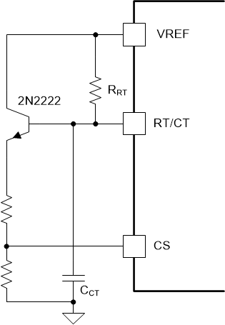
Implementation of voltage mode control is possible by using a fraction of the oscillator timing capacitor (CCT) waveform. This value can be divided down and fed to the current sense pin as shown in Figure 7-9. The oscillator timing components must be selected to approximate as close to a linear sawtooth waveform as possible. Although exponentially charged, large values of timing resistance and small values of timing capacitance help approximate a more linear shaped waveform. A small transistor is used to buffer the oscillator timing components from the loading of the resistive divider network. Due to the offset of the oscillator’s lower timing threshold, a DC blocking capacitor is added.
 Figure 7-9 Current Mode PWM Used as a Voltage Mode PWM