SLUS458I July 2000 – June 2024 UCC28C40 , UCC28C41 , UCC28C42 , UCC28C43 , UCC28C44 , UCC28C45 , UCC38C40 , UCC38C41 , UCC38C42 , UCC38C43 , UCC38C44 , UCC38C45
PRODUCTION DATA
- 1
- 1 Features
- 2 Applications
- 3 Description
- 4 Device Comparison Table
- 5 Pin Configuration and Functions
- 6 Specifications
-
7 Detailed Description
- 7.1 Overview
- 7.2 Functional Block Diagram
- 7.3
Feature Description
- 7.3.1 Detailed Pin Description
- 7.3.2 Undervoltage Lockout
- 7.3.3 ±1% Internal Reference Voltage
- 7.3.4 Current Sense and Overcurrent Limit
- 7.3.5 Reduced-Discharge Current Variation
- 7.3.6 Oscillator Synchronization
- 7.3.7 Soft-Start Timing
- 7.3.8 Enable and Disable
- 7.3.9 Slope Compensation
- 7.3.10 Voltage Mode
- 7.4 Device Functional Modes
-
8 Application and Implementation
- 8.1 Application Information
- 8.2
Typical Application
- 8.2.1 Design Requirements
- 8.2.2
Detailed Design Procedure
- 8.2.2.1 Input Bulk Capacitor and Minimum Bulk Voltage
- 8.2.2.2 Transformer Turns Ratio and Maximum Duty Cycle
- 8.2.2.3 Transformer Inductance and Peak Currents
- 8.2.2.4 Output Capacitor
- 8.2.2.5 Current Sensing Network
- 8.2.2.6 Gate Drive Resistor
- 8.2.2.7 VREF Capacitor
- 8.2.2.8 RT/CT
- 8.2.2.9 Start-Up Circuit
- 8.2.2.10 Voltage Feedback Compensation
- 8.2.3 Application Curves
- 8.3 Power Supply Recommendations
- 8.4 Layout
- 9 Device and Documentation Support
- 10Revision History
- 11Mechanical, Packaging, and Orderable Information
Package Options
Refer to the PDF data sheet for device specific package drawings
Mechanical Data (Package|Pins)
- D|8
- DGK|8
Thermal pad, mechanical data (Package|Pins)
Orderable Information
7.3.2 Undervoltage Lockout
Six sets of UVLO thresholds are available with turn-on and turnoff thresholds of: (14.5V and 9V), (8.4V and 7.6V), (7V and 6.6V) respectively. The first set is primarily intended for off-line and 48V distributed power applications, where the wider hysteresis allows for lower frequency operation and longer soft-starting time of the converter. The second group of UVLO options is ideal for high frequency DC-DC converters typically running from a 12VDC input. The third, and newest, set has been added to address battery powered and portable applications. Table 7-2 shows the maximum duty cycle and UVLO thresholds by device.
| MAXIMUM DUTY CYCLE (%) | UVLO ON (V) | UVLO OFF (V) | DEVICE NUMBER |
|---|---|---|---|
| 100 | 14.5 | 9 | UCCx8C42 |
| 100 | 8.4 | 7.6 | UCCx8C43 |
| 100 | 7 | 6.6 | UCCx8C40 |
| 50 | 14.5 | 9 | UCCx8C44 |
| 50 | 8.4 | 7.6 | UCCx8C45 |
| 50 | 7 | 6.6 | UCCx8C41 |
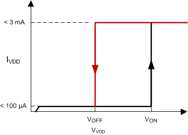
During UVLO the IC draws less than 100µA of supply current. After crossing the turnon threshold, the device supply current increases to a maximum of 3mA, typically 2.3mA. This low start-up current allows the power supply designer to optimize the selection of the startup resistor value to provide a more efficient design. In applications where low component cost overrides maximum efficiency, the low run current of 2.3mA (typical) allows the control device to run directly through the single resistor to (+) rail, rather than requiring a bootstrap winding on the power transformer, along with a rectifier. The start and run resistor for this case must also pass enough current to allow driving the primary switching MOSFET, which may be a few milliamps in small devices.
 Figure 7-2 UVLO ON and OFF Profile