SLUS458I July 2000 – June 2024 UCC28C40 , UCC28C41 , UCC28C42 , UCC28C43 , UCC28C44 , UCC28C45 , UCC38C40 , UCC38C41 , UCC38C42 , UCC38C43 , UCC38C44 , UCC38C45
PRODUCTION DATA
- 1
- 1 Features
- 2 Applications
- 3 Description
- 4 Device Comparison Table
- 5 Pin Configuration and Functions
- 6 Specifications
-
7 Detailed Description
- 7.1 Overview
- 7.2 Functional Block Diagram
- 7.3
Feature Description
- 7.3.1 Detailed Pin Description
- 7.3.2 Undervoltage Lockout
- 7.3.3 ±1% Internal Reference Voltage
- 7.3.4 Current Sense and Overcurrent Limit
- 7.3.5 Reduced-Discharge Current Variation
- 7.3.6 Oscillator Synchronization
- 7.3.7 Soft-Start Timing
- 7.3.8 Enable and Disable
- 7.3.9 Slope Compensation
- 7.3.10 Voltage Mode
- 7.4 Device Functional Modes
-
8 Application and Implementation
- 8.1 Application Information
- 8.2
Typical Application
- 8.2.1 Design Requirements
- 8.2.2
Detailed Design Procedure
- 8.2.2.1 Input Bulk Capacitor and Minimum Bulk Voltage
- 8.2.2.2 Transformer Turns Ratio and Maximum Duty Cycle
- 8.2.2.3 Transformer Inductance and Peak Currents
- 8.2.2.4 Output Capacitor
- 8.2.2.5 Current Sensing Network
- 8.2.2.6 Gate Drive Resistor
- 8.2.2.7 VREF Capacitor
- 8.2.2.8 RT/CT
- 8.2.2.9 Start-Up Circuit
- 8.2.2.10 Voltage Feedback Compensation
- 8.2.3 Application Curves
- 8.3 Power Supply Recommendations
- 8.4 Layout
- 9 Device and Documentation Support
- 10Revision History
- 11Mechanical, Packaging, and Orderable Information
Package Options
Refer to the PDF data sheet for device specific package drawings
Mechanical Data (Package|Pins)
- D|8
- P|8
- DGK|8
Thermal pad, mechanical data (Package|Pins)
Orderable Information
8.2.2.10.3 Open-Loop Gain
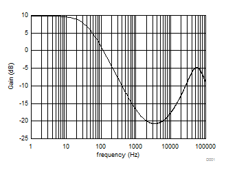
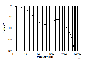
Once the power stage poles and zeros are calculated and the slope compensation is determined, the power stage open-loop gain and phase of the CCM flyback converter can be plotted as a function of frequency. The power stage transfer function can be characterized with Equation 39.
Equation 39. 

The bode for the open-loop gain and phase can be plotted by using Equation 40.
Equation 40. 

See Figure 8-4 and Figure 8-5.
 Figure 8-4 Converter Open-Loop Bode Plot - Gain
 Figure 8-5 Converter Open-Loop Bode Plot - Phase