SLUS495J August 2001 – December 2023 UCC29002 , UCC39002
PRODUCTION DATA
- 1
- 1Features
- 2Applications
- 3Description
- 4Pin Configuration and Functions
- 5Specifications
-
6Detailed Description
- 6.1 Overview
- 6.2 Functional Block Diagram
- 6.3
Feature Description
- 6.3.1 Differential Current-Sense Amplifier (CS+, CS−, CSO)
- 6.3.2 Load-Share Bus Driver Amplifier (CSO, LS)
- 6.3.3 Load-Share Bus Receiver Amplifier (LS)
- 6.3.4 Error Amplifier (EAO)
- 6.3.5 Adjust Amplifier Output (ADJ)
- 6.3.6 Enable Function (CS+, CS−)
- 6.3.7 Fault Protection on LS Bus
- 6.3.8 Start-Up and Adjust Logic
- 6.3.9 Bias Input and Bias_OK Circuit (VDD)
- 6.4 Device Functional Modes
- 7Application and Implementation
- 8Device and Documentation Support
- 9Revision History
- Mechanical, Packaging, and Orderable Information
Package Options
Mechanical Data (Package|Pins)
Thermal pad, mechanical data (Package|Pins)
Orderable Information
7.2 Paralleling the Power Modules
The symbols used in this section are defined as:
- VOUTThe nominal output voltage of the modules to be paralleled.
- IOUT(max)The maximum output current of each module to be paralleled.
- ΔVADJ(max) The maximum output voltage adjustment range of the power modules to be paralleled.
- NmThe number of power modules to be paralleled.
The power modules to be paralleled must be equipped with true remote-sense inputs or with access to the feedback divider network of the module’s error amplifier.
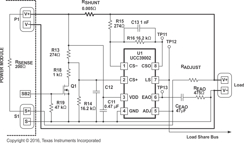
Figure 7-1 shows a typical high-side current-sense configuration for a single module which is repeated for each module to be paralleled. Direct connection of the VDD pin to the power module VOUT rail (V+) is valid for VOUT less than 13.5V.
 Figure 7-1 Typical
High-Side Application for a Single Power Module
Figure 7-1 Typical
High-Side Application for a Single Power ModuleIn Figure 7-1, P1 represents the output-voltage connector terminals of the module and S1 represents the remote-sense connector terminals of the module. In this example, a signal on the SB2 terminal enables the disconnect feature of the device. The Load-Share Bus is the common bus between all of the paralleled load-share controllers. The VDD supply must be decoupled with a good-quality ceramic capacitor returned directly to GND.
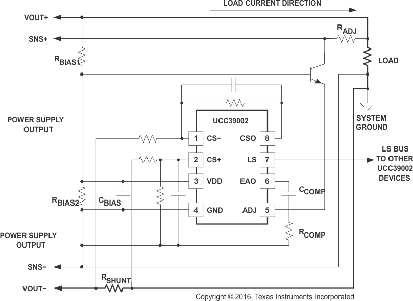
For applications where the module output voltage is higher than the maximum VDD rating, it is best practice to configure RSHUNT in the GND-return rail as shown in Figure 7-2. The VCC pin is biased from VOUT using dropping resistor RBIAS1 to limit current and the ADJ pin is buffered from VOUT by an NPN transistor.
 Figure 7-2 High-Voltage Application with Low-side Current-Sensing