SLUSE29F May   2020  – July 2024 UCC5350-Q1

PRODUCTION DATA  

  1.   1
  2. Features
  3. Applications
  4. Description
  5. Description (continued)
  6. Pin Configuration and Function
  7. Specifications
    1. 6.1  Absolute Maximum Ratings
    2. 6.2  ESD Ratings
    3. 6.3  Recommended Operating Conditions
    4. 6.4  Thermal Information
    5. 6.5  Power Ratings
    6. 6.6  Insulation Specifications for D Package
    7. 6.7  Insulation Specifications for DWV Package
    8. 6.8  Safety-Related Certifications For D Package
    9. 6.9  Safety-Related Certifications For DWV Package
    10. 6.10 Safety Limiting Values
    11. 6.11 Electrical Characteristics
    12. 6.12 Switching Characteristics
    13. 6.13 Insulation Characteristics Curves
    14. 6.14 Typical Characteristics
  8. Parameter Measurement Information
    1. 7.1 Propagation Delay, Inverting, and Noninverting Configuration
      1. 7.1.1 CMTI Testing
  9. Detailed Description
    1. 8.1 Overview
    2. 8.2 Functional Block Diagram
    3. 8.3 Feature Description
      1. 8.3.1 Power Supply
      2. 8.3.2 Input Stage
      3. 8.3.3 Output Stage
      4. 8.3.4 Protection Features
        1. 8.3.4.1 Undervoltage Lockout (UVLO)
        2. 8.3.4.2 Active Pulldown
        3. 8.3.4.3 Short-Circuit Clamping
        4. 8.3.4.4 Active Miller Clamp
    4. 8.4 Device Functional Modes
      1. 8.4.1 ESD Structure
  10. Application and Implementation
    1. 9.1 Application Information
    2. 9.2 Typical Application
      1. 9.2.1 Design Requirements
      2. 9.2.2 Detailed Design Procedure
        1. 9.2.2.1 Designing IN+ and IN– Input Filter
        2. 9.2.2.2 Gate-Driver Output Resistor
        3. 9.2.2.3 Estimate Gate-Driver Power Loss
        4. 9.2.2.4 Estimating Junction Temperature
      3. 9.2.3 Selecting VCC1 and VCC2 Capacitors
        1. 9.2.3.1 Selecting a VCC1 Capacitor
        2. 9.2.3.2 Selecting a VCC2 Capacitor
        3. 9.2.3.3 Application Circuits with Output Stage Negative Bias
      4. 9.2.4 Application Curve
  11. 10Power Supply Recommendations
  12. 11Layout
    1. 11.1 Layout Guidelines
    2. 11.2 Layout Example
    3. 11.3 PCB Material
  13. 12Device and Documentation Support
    1. 12.1 Device Support
      1. 12.1.1 Third-Party Products Disclaimer
    2. 12.2 Documentation Support
      1. 12.2.1 Related Documentation
    3. 12.3 Certifications
    4. 12.4 Receiving Notification of Documentation Updates
    5. 12.5 Support Resources
    6. 12.6 Trademarks
    7. 12.7 Electrostatic Discharge Caution
    8. 12.8 Glossary
  14. 13Revision History
  15. 14Mechanical, Packaging, and Orderable Information

Package Options

Mechanical Data (Package|Pins)
Thermal pad, mechanical data (Package|Pins)
Orderable Information

Functional Block Diagram

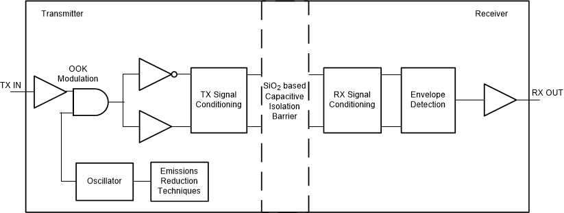
UCC5350-Q1 Conceptual Block Diagram of a Capacitive Data
                                                  Channel Figure 8-1 Conceptual Block Diagram of a Capacitive Data Channel
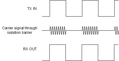
UCC5350-Q1 On-Off Keying (OOK) Based Modulation
                                                  Scheme Figure 8-2 On-Off Keying (OOK) Based Modulation Scheme
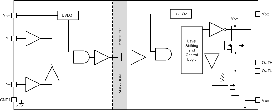
UCC5350-Q1 Functional Block Diagram — Split Output Figure 8-3 Functional Block Diagram — Split Output
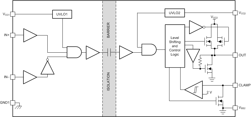
UCC5350-Q1 Functional Block Diagram — Miller Clamp Figure 8-4 Functional Block Diagram — Miller Clamp