SLUSDR3B June 2019 – February 2024 UCC5390-Q1
PRODUCTION DATA
- 1
- 1 Features
- 2 Applications
- 3 Description
- 4 Pin Configuration and Function
-
5 Specifications
- 5.1 Absolute Maximum Ratings
- 5.2 ESD Ratings
- 5.3 Recommended Operating Conditions
- 5.4 Thermal Information
- 5.5 Power Ratings
- 5.6 Insulation Specifications for DWV Package
- 5.7 Safety-Related Certifications For DWV Package
- 5.8 Safety Limiting Values
- 5.9 Electrical Characteristics
- 5.10 Switching Characteristics
- 5.11 Insulation Characteristics Curves
- 5.12 Typical Characteristics
- 6 Parameter Measurement Information
- 7 Detailed Description
- 8 Application and Implementation
- 9 Power Supply Recommendations
- 10Layout
- 11Device and Documentation Support
- 12Revision History
- 13Mechanical, Packaging, and Orderable Information
Package Options
Mechanical Data (Package|Pins)
- DWV|8
Thermal pad, mechanical data (Package|Pins)
Orderable Information
3 Description
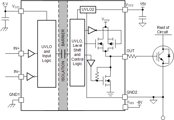
The UCC5390-Q1 is a single-channel, isolated gate driver with 10A source and 10A sink peak current designed to drive MOSFETs, IGBTs, and SiC MOSFETs. The UCC5390-Q1 has its UVLO2 referenced to GND2, which facilitates bipolar supplies and optimizes SiC and IGBT switching behavior and robustness.
The UCC5390-Q1 is available in 8.5mm SOIC-8 (DWV) package and can support isolation voltage up to 5kVRMS. The input side is isolated from the output side with SiO2 capacitive isolation technology with longer than 40 years isolation barrier lifetime. With its high drive strength and true UVLO detection, this device is a good fit for driving IGBTs and SiC MOSFETs in applications such as on-board chargers and traction inverters.
Compared to an optocoupler, the UCC5390-Q1 has lower part-to-part skew, lower propagation delay, higher operating temperature, and higher CMTI.
| PART VERSION | PACKAGE(1) | BODY SIZE (NOM) |
|---|---|---|
| UCC5390-Q1 | DWV (SOIC-8) | 7.5mm × 5.85mm |
 Functional Block Diagram