SLUSFL3B June   2024  – October 2024 UCC57102 , UCC57108

PRODUCTION DATA  

  1.   1
  2. Features
  3. Applications
  4. Description
  5. Pin Configuration and Functions
  6. Specifications
    1. 5.1 Absolute Maximum Ratings
    2. 5.2 ESD Ratings
    3. 5.3 Thermal Information
    4. 5.4 Recommended Operating Conditions
    5. 5.5 Electrical Characteristics
    6. 5.6 Switching Characteristics
    7. 5.7 Timing Diagrams
    8. 5.8 Typical Characteristics
  7. Detailed Description
    1. 6.1 Overview
    2. 6.2 Functional Block Diagram
    3. 6.3 Feature Description
      1. 6.3.1 Input Stage
      2. 6.3.2 Enable Function
      3. 6.3.3 Driver Stage
      4. 6.3.4 Desaturation (DESAT) Protection
      5. 6.3.5 Fault (FLT)
      6. 6.3.6 VREF
      7. 6.3.7 Thermal Shutdown
    4. 6.4 Device Functional Modes
  8. Applications and Implementation
    1. 7.1 Application Information
    2. 7.2 Typical Application
      1. 7.2.1 Design Requirements
      2. 7.2.2 Detailed Design Procedure
        1. 7.2.2.1 VDD Undervoltage Lockout
      3. 7.2.3 Application Curves
  9. Power Supply Recommendations
  10. Layout
    1. 9.1 Layout Guidelines
    2. 9.2 Layout Example
  11. 10Device and Documentation Support
    1. 10.1 Third-Party Products Disclaimer
    2. 10.2 Receiving Notification of Documentation Updates
    3. 10.3 Support Resources
    4. 10.4 Trademarks
    5. 10.5 Electrostatic Discharge Caution
    6. 10.6 Glossary
  12. 11Revision History
  13. 12Mechanical, Packaging, and Orderable Information

Package Options

Refer to the PDF data sheet for device specific package drawings

Mechanical Data (Package|Pins)
  • D|8
Thermal pad, mechanical data (Package|Pins)
Orderable Information

Typical Characteristics

Unless otherwise specified, VDD=15V, VEE=0V, IN=3.3V, EN=5V, TJ = 25 °C, No load
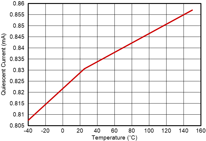
UCC57108 UCC57102 Quiescent Current
VDD = 6.5V
Figure 5-5 Quiescent Current
UCC57108 UCC57102 Disable Current
Figure 5-7 Disable Current
UCC57108 UCC57102 UVLO Threshold Figure 5-9 UVLO Threshold
UCC57108 UCC57102 Input Pulldown ResistanceFigure 5-11 Input Pulldown Resistance
UCC57108 UCC57102 Enable Up ResistanceFigure 5-13 Enable Up Resistance
UCC57108 UCC57102 Output Pulldown Resistance Figure 5-15 Output Pulldown Resistance
UCC57108 UCC57102 Output Fall Time
CLOAD = 1.8 nF
Figure 5-17 Output Fall Time
UCC57108 UCC57102 Input
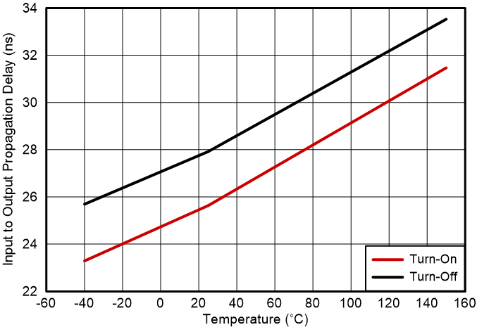
                        to Output Rising (Turnon) Propagation Delay
CLOAD = 1.8 nF
Figure 5-19 Input to Output Rising (Turnon) Propagation Delay
UCC57108 UCC57102 Input Propagation Delay
CLOAD = 1.8 nF
Figure 5-21 Input Propagation Delay
UCC57108 UCC57102 Vref
                        Voltage vs VDDFigure 5-23 Vref Voltage vs VDD
UCC57108 UCC57102 Soft
                        Turn Off Pulldown Resistance vs VDDFigure 5-25 Soft Turn Off Pulldown Resistance vs VDD
UCC57108 UCC57102 DESAT Threshold vs Temperature Figure 5-27 DESAT Threshold vs Temperature
UCC57108 UCC57102 FLTb
                        vs Temperature
IFLTb_sink = 15mA
Figure 5-29 FLTb vs Temperature
UCC57108 UCC57102 Operating Static Supply Current
Figure 5-6 Operating Static Supply Current
UCC57108 UCC57102 Operating Supply Current
CLOAD = 1.8 nF
Figure 5-8 Operating Supply Current
UCC57108 UCC57102 Input Threshold Figure 5-10 Input Threshold
UCC57108 UCC57102 Enable Threshold Figure 5-12 Enable Threshold
UCC57108 UCC57102 Output Pullup Resistance vs VDDFigure 5-14 Output Pullup Resistance vs VDD
UCC57108 UCC57102 Output Rise Time
CLOAD = 1.8 nF
Figure 5-16 Output Rise Time
UCC57108 UCC57102 Output Rise and Fall Time
CLOAD = 1.8 nF
Figure 5-18 Output Rise and Fall Time
UCC57108 UCC57102 Input
                        to Output Falling (Turnoff) Propagation Delay
CLOAD = 1.8 nF
Figure 5-20 Input to Output Falling (Turnoff) Propagation Delay
UCC57108 UCC57102 Enable Propagation Delay
CLOAD = 1.8 nF
Figure 5-22 Enable Propagation Delay
UCC57108 UCC57102 Vref Voltage vs
                        TemperatureFigure 5-24 Vref Voltage vs Temperature
UCC57108 UCC57102 DESAT Charge Current
                        vs TemperatureFigure 5-26 DESAT Charge Current vs Temperature
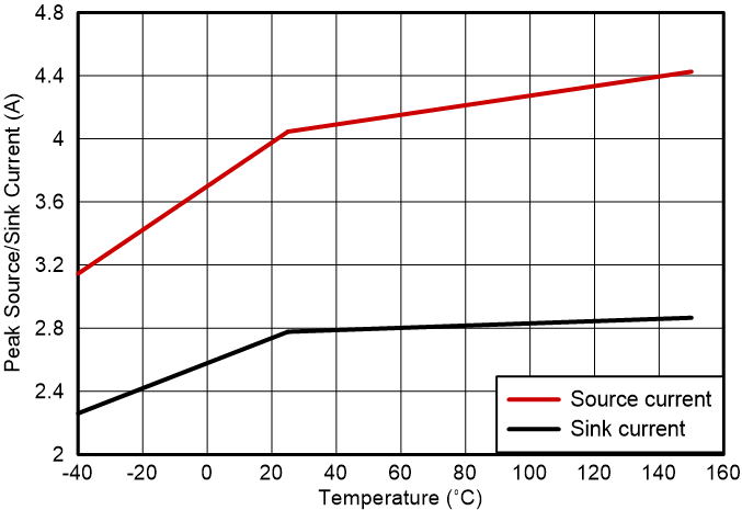
UCC57108 UCC57102 Peak
                        Source and Sink Current
CLOAD = 100 nF
Figure 5-28 Peak Source and Sink Current