SLUSB72D March 2013 – April 2021 UCD3138064
PRODUCTION DATA
- 1 Features
- 2 Applications
- 3 Description
- 4 Functional Block Diagram
- 5 Revision History
- 6 Device Options
- 7 Pin Configuration and Functions
-
8 Specifications
- 8.1 Absolute Maximum Ratings (1)
- 8.2 Handling Ratings
- 8.3 Recommended Operating Conditions
- 8.4 Thermal Information
- 8.5 Electrical Characteristics
- 8.6 Timing Characteristics
- 8.7 PMBus/SMBus/I2C Timing
- 8.8 Power On Reset (POR) / Brown Out Reset (BOR)
- 8.9 Typical Clock Gating Power Savings
- 8.10 Typical Characteristics
-
9 Detailed Description
- 9.1 Overview
- 9.2 Functional Block Diagram
- 9.3
Feature Description
- 9.3.1 System Module
- 9.3.2 Peripherals
- 9.3.3 Automatic Mode Switching
- 9.3.4 DPWMC, Edge Generation, Intramux
- 9.3.5 Filter
- 9.3.6 Communication Ports
- 9.3.7 Real Time Clock
- 9.3.8 Timers
- 9.3.9 General Purpose ADC12
- 9.3.10 Miscellaneous Analog
- 9.3.11 Brownout
- 9.3.12 Global I/O
- 9.3.13 Temperature Sensor Control
- 9.3.14 I/O Mux Control
- 9.3.15 Current Sharing Control
- 9.3.16 Temperature Reference
- 9.4 Device Functional Modes
- 9.5 Memory
-
10Applications and
Implementation
- 10.1 Application Information
- 10.2
Typical Application
- 10.2.1 Design Requirements
- 10.2.2 Detailed Design Procedure
- 10.2.3 Application Curves
- 11Power Supply Recommendations
- 12Layout
- 13Device and Documentation Support
- 14Mechanical, Packaging, and Orderable Information
Package Options
Mechanical Data (Package|Pins)
Thermal pad, mechanical data (Package|Pins)
Orderable Information
8.7 PMBus/SMBus/I2C Timing
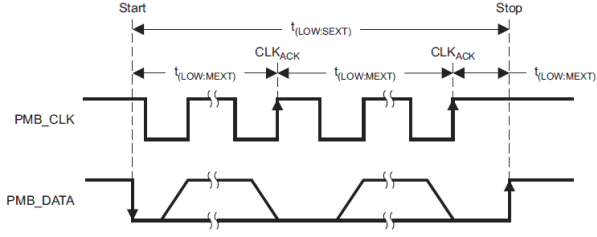
The timing characteristics and timing diagram for the communications interface that supports I2C, SMBus, and PMBus in Slave or Master mode are shown in Table 8-1, Figure 8-1, and Figure 8-2. The numbers in Table 8-1 are for 400 kHz operating frequency. However, the device supports all three speeds, standard (100 kHz), fast (400 kHz), and fast mode plus (1 MHz).
Table 8-1 I2C/SMBus/PMBus Timing Characteristics
| PARAMETER | TEST CONDITIONS | MIN | TYP | MAX | UNIT | |
|---|---|---|---|---|---|---|
| Typical values at TA = 25 °C and VCC = 3.3 V (unless otherwise noted) | ||||||
| fSMB | SMBus/PMBus operating frequency | Slave mode, SMBC 50% duty cycle | 100 | 400 | kHz | |
| fI2C | I2C operating frequency | Slave mode, SCL 50% duty cycle | 100 | 400 | kHz | |
| t(BUF) | Bus free time between start and stop(5) | 1.3 | µs | |||
| t(HD:STA) | Hold time after (repeated) start(5) | 0.6 | µs | |||
| t(SU:STA) | Repeated start setup time(5) | 0.6 | µs | |||
| t(SU:STO) | Stop setup time(5) | 0.6 | µs | |||
| t(HD:DAT) | Data hold time | Receive mode | 0 | ns | ||
| t(SU:DAT) | Data setup time | 100 | ns | |||
| t(TIMEOUT) | Error signal/detect(1) | 35 | ms | |||
| t(LOW) | Clock low period | 1.3 | µs | |||
| t(HIGH) | Clock high period(2) | 0.6 | 50 | µs | ||
| t(LOW:SEXT) | Cumulative clock low slave extend time(3) | 25 | ms | |||
| tf | Clock/data fall time | Fall time tf = 0.9 VDD to (VILmax – 0.15) | 20 + 0.1 Cb(4) | 300 | ns | |
| tr | Clock/data rise time | Rise time tr = (VILmax – 0.15) to (VIHmin + 0.15) | 20 + 0.1 Cb(4) | 300 | ns | |
| Cb | Total capacitance of one bus line | 400 | pF | |||
(1) The device times out when any clock low exceeds t(TIMEOUT).
(2) t(HIGH), Max, is the minimum bus idle time. SMBC = SMBD = 1 for t > 50 ms causes reset of any transaction that is in progress. This specification is valid when the NC_SMB control bit remains in the default cleared state (CLK[0] = 0).
(3) t(LOW:SEXT) is the cumulative time a slave device is allowed to extend the clock cycles in one message from initial start to the stop.
(4) Cb (pF)
(5) Fast mode, 400 kHz
 Figure 8-1 I2C/SMBus/PMBus Timing Diagram
 Figure 8-2 Bus Timing in Extended Mode