SLUS645F February 2005 – December 2014 UCD7201
PRODUCTION DATA.
- 1 Features
- 2 Applications
- 3 Description
- 4 Revision History
- 5 Description (Continued)
- 6 Pin Configuration and Functions
- 7 Specifications
- 8 Detailed Description
- 9 Applications and Implementation
- 10Power Supply Recommendations
- 11Layout
- 12Device and Documentation Support
- 13Mechanical, Packaging, and Orderable Information
Package Options
Mechanical Data (Package|Pins)
- PWP|14
Thermal pad, mechanical data (Package|Pins)
Orderable Information
8 Detailed Description
8.1 Overview
The UCD7201 is a member of the UCD7K family of digital control compatible drivers for applications utilizing digital control techniques or applications requiring fast local peak current limit protection.
The UCD7201 is a low-side ±4-A high-current MOSFET gate driver. It allows the digital power controllers such as UCD9110 or UCD9501 to interface to the power stage in double ended topologies. It provides a cycle-by-cycle current limit function for both driver channels, a programmable threshold and a digital output current limit flag which can be monitored by the host controller. With a fast cycle-by-cycle current limit protection, the driver can turn off the power stage in the event of an overcurrent condition.
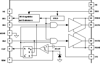
8.2 Functional Block Diagram
8.3 Feature Description
8.3.1 Reference / External Bias Supply
All devices in the UCD7K family are capable of supplying a regulated 3.3-V rail to power various types of external loads such as a microcontroller or an ASIC. The onboard linear voltage regulator is capable of sourcing up to 10 mA of current. For normal operation, place 0.22-μF of ceramic capacitance between the 3V3 pin to the AGND pin.
8.3.2 Input Pin
The input pins are high impedance digital inputs capable of accepting 3.3-V logic level signals up to 2 MHz. There is an internal Schmitt Trigger comparator which isolates the internal circuitry from any external noise.
If limiting the rise or fall times to the power device is desired then an external resistance may be added between the output of the driver and the load device, which is generally the gate of a power MOSFET.
8.3.3 Current Sensing and Protection
A very fast current limit comparator connected to the CS pin is used to protect the power stage by implementing cycle-by-cycle current limiting.
The current limit threshold may be set to any value between 0.25 V and 1.0 V by applying the desired threshold voltage to the current limit (ILIM) pin. If the ILIM pin is left floating, the internal current limit threshold will be 0.5 volts. When the CS level is greater than the ILIM voltage minus 25 mV, the output of the driver is forced low and the current limit flag (CLF) is set high. The CLF signal is latched high until the device receives the next rising edge on either of the IN pins.
When the CS voltage is below ILIM, the driver output follows the PWM input. The CLF digital output flag can be monitored by the host controller to determine when a current limit event occurs and to then apply the appropriate algorithm to obtain the desired current limit profile (i.e. straight time, fold back, hickup or latch-off).
A benefit of this local protection feature is that the UCD7K devices can protect the power stage if the software code in the digital controller becomes corrupted. If the controller’s PWM output stays high, the local current sense circuit turns off the driver output when an over-current event occurs. The system would then likely go into retry mode because most DSP and microcontrollers have on-board watchdog, brown-out, and other supervisory peripherals to restart the device in the event that it is not operating properly. But these peripherals typically do not react fast enough to save the power stage. The UCD7K’s local current limit comparator provides the required fast protection for the power stage.
The CS threshold is 25 mV below the ILIM voltage. If the user attempts to command zero current while the CS pin is at ground the CLF flag will latch high until the IN pin receives a pulse. At start-up it is necessary to ensure that the ILIM pin will always be greater than the CS pin for the handshaking to work as described below. If for any reason the CS pin comes to within 25 mV of the ILIM pin during start-up, then the CLF flag will be latched high and the digital controller must poll the UCD7K device, by sending it a narrow IN pulse. If a fault condition is not present the IN pulse will reset the CLF signal to low indicating that the UCD7K device is ready to process power pulses.
8.3.4 Handshaking
The UCD7K family of devices have a built-in handshaking feature to facilitate efficient start-up of the digitally controlled power supply. At start-up the CLF flag is held high until all the internal and external supply voltages of the UCD7K device are within their operating range. Once the supply voltages are within acceptable limits, the CLF goes low and the device will process input drive signals. The micro-controller should monitor the CFL flag at start-up and wait for the CLF flag to go LOW before sending power pulses to the UCD7K device.
8.3.5 Driver Output
The high-current output stage of the UCD7K device family is capable of supplying ±4-A peak current pulses and swings to both PVDD and PGND. The driver outputs follow the state of the IN pin provided that the VDD and 3V3 voltages are above their respective under-voltage lockout threshold.
The drive output utilizes Texas Instruments' TrueDrive™ architecture, which delivers rated current into the gate of a MOSFET when it is most needed, during the Miller plateau region of the switching transition providing efficiency gains.
TrueDrive™ consists of pullup pulldown circuits with bipolar and MOSFET transistors in parallel. The peak output current rating is the combined current from the bipolar and MOSFET transistors. This hybrid output stage also allows efficient current sourcing at low supply voltages.
Each output stage also provides a very low impedance to overshoot and undershoot due to the body diode of the external MOSFET. This means that in many cases, external-schottky-clamp diodes are not required.
8.3.6 Source/Sink Capabilities During Miller Plateau
Large power MOSFETs present a large load to the control circuitry. Proper drive is required for efficient, reliable operation. The UCD7K drivers have been optimized to provide maximum drive to a power MOSFET during the Miller plateau region of the switching transition. This interval occurs while the drain voltage is swinging between the voltage levels dictated by the power topology, requiring the charging/discharging of the drain-gate capacitance with current supplied or removed by the driver device. See Reference [1]
8.3.7 Drive Current and Power Requirements
The UCD7K family of drivers can deliver high current into a MOSFET gate for a period of several hundred nanoseconds. High peak current is required to turn the device ON quickly. Then, to turn the device OFF, the driver is required to sink a similar amount of current to ground. This repeats at the operating frequency of the power device.
Reference [1] discusses the current required to drive a power MOSFET and other capacitive-input switching devices.
When a driver device is tested with a discrete, capacitive load it is a fairly simple matter to calculate the power that is required from the bias supply. The energy that must be transferred from the bias supply to charge the capacitor is given by:

where C is the load capacitor and V is the bias voltage feeding the driver.
There is an equal amount of energy transferred to ground when the capacitor is discharged. This leads to a power loss given by the following:

where f is the switching frequency.
This power is dissipated in the resistive elements of the circuit. Thus, with no external resistor between the driver and gate, this power is dissipated inside the driver. Half of the total power is dissipated when the capacitor is charged, and the other half is dissipated when the capacitor is discharged.
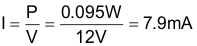
With VDD = 12 V, CLOAD = 2.2 nF, and f = 300 kHz, the power loss can be calculated as:

With a 12-V supply, this would equate to a current of:
8.3.8 Operational Waveforms
Figure 22 shows the circuit performance achievable with the output driving a 10-nF load at 12-V VDD. The input pulsewidth (not shown) is set to 200 ns to show both transitions in the output waveform. Note the linear rising and falling edges of the switching waveforms. This is due to the constant output current characteristic of TrueDrive™ stage as opposed to the resistive output impedance of traditional MOSFET-based gate drivers.
8.4 Device Functional Modes
8.4.1 Operation with VDD < 4.25 V (Minimum VDD)
The devices operate with VDD voltages above 4.75 V. The maximum UVLO voltage is 4.75 V and operates at VDD voltages above 4.75 V. The typical UVLO voltage is 4.5 V. The minimum UVLO voltage is 4.25 V. At VDD below the actual UVLO voltage, the devices do not operate, OUT1 and OUT2 remain low.
8.4.2 Operation with IN Pin Open
If the IN1 or IN2 pin is disconnected (open), a 100 kΩ internal resistor connects IN1 or IN2 to GND to prevent unpredictable operation due to a floating IN1 or IN2 pin, OUT1 or OUT2 remains low.
8.4.3 Operation with ILIM Pin Open
If the ILIM pin is disconnected (open), the current limit threshold is set at 0.55 V.
8.4.4 Operation with ILIM Pin High
If the signal on ILIM pin is higher than 1.1 V, the current limit threshold is clamped at 1.1 V.