SLUS645F February 2005 – December 2014 UCD7201
PRODUCTION DATA.
- 1 Features
- 2 Applications
- 3 Description
- 4 Revision History
- 5 Description (Continued)
- 6 Pin Configuration and Functions
- 7 Specifications
- 8 Detailed Description
- 9 Applications and Implementation
- 10Power Supply Recommendations
- 11Layout
- 12Device and Documentation Support
- 13Mechanical, Packaging, and Orderable Information
Package Options
Mechanical Data (Package|Pins)
- PWP|14
Thermal pad, mechanical data (Package|Pins)
Orderable Information
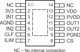
6 Pin Configuration and Functions
PWP
14 PIN
Top View

Pin Functions
| PIN | I/O | FUNCTION | |
|---|---|---|---|
| NO. | NAME | ||
| 1 | NC | - | No Connection |
| 2 | 3V3 | O | Regulated 3.3-V rail. The onboard linear voltage regulator is capable of sourcing up to 10 mA of current. Place 0.22 μF of ceramic capacitance from this pin to ground. |
| 3 | IN1 | I | The IN pin is a high impedance digital input capable of accepting 3.3-V logic level signals up to 2 MHz. There is an internal Schmitt trigger comparator which isolates the internal circuitry from any external noise. |
| 4 | AGND | - | Analog ground return. |
| 5 | IN2 | I | The IN pin is a high impedance digital input capable of accepting 3.3-V logic level signals up to 2 MHz. There is an internal Schmitt trigger comparator which isolates the internal circuitry from any external noise. |
| 6 | CLF | O | Current limit flag. When the CS level is greater than the ILIM voltage minus 25 mV, the output of the driver is forced low and the current limit flag (CLF) is set high. The CLF signal is latched high until the device receives the next rising edge on the IN pin. |
| 7 | ILIM | I | Current limit threshold set pin. The current limit threshold can be set to any value between 0.25 V and 1.0 V. The default value while open is 0.5 V. |
| 8 | CS | I | Current sense pin. Fast current limit comparator connected to the CS pin is used to protect the power stage by implementing cycle-by-cycle current limiting. |
| 9 | PGND | - | Power ground return. The pin should be connected very closely to the source of the power MOSFET. |
| 10 | OUT2 | O | The high-current TrueDrive™ driver output. |
| 11 | OUT1 | O | The high-current TrueDrive™ driver output. |
| 12 | PVDD | I | Supply pin provides power for the output drivers. It is not connected internally to the VDD supply rail. The bypass capacitor for this pin should be returned to PGND. |
| 13 | VDD | I | Supply input pin to power the driver. The UCD7K devices accept an input range of 4.5 V to 15 V. Bypass the pin with at least 4.7 μF of capacitance, returned to AGND. |
| 14 | NC | - | No Connection. |