SLVSDD4C September   2016  – March 2020 UCD90160A

PRODUCTION DATA.  

  1. Features
  2. Applications
  3. Description
    1.     Simplified Application
  4. Revision History
  5. Pin Configuration and Functions
    1.     Pin Functions
  6. Specifications
    1. 6.1 Absolute Maximum Ratings
    2. 6.2 ESD Ratings
    3. 6.3 Recommended Operating Conditions
    4. 6.4 Thermal Information
    5. 6.5 Electrical Characteristics
    6. 6.6 Timing Requirements
    7. 6.7 Typical Characteristics
  7. Detailed Description
    1. 7.1 Overview
    2. 7.2 Functional Block Diagram
    3. 7.3 Feature Description
      1. 7.3.1 Rail Configuration
      2. 7.3.2 TI Fusion GUI
      3. 7.3.3 PMBus Interface
    4. 7.4 Device Functional Modes
      1. 7.4.1  Power Supply Sequencing
        1. 7.4.1.1 Turn-on Sequencing
        2. 7.4.1.2 Turn-off Sequencing
        3. 7.4.1.3 Sequencing Configuration Options
      2. 7.4.2  Pin-Selected Rail States
      3. 7.4.3  Voltage Monitoring
      4. 7.4.4  Fault Responses and Alert Processing
      5. 7.4.5  Shut Down All Rails and Sequence On (Resequence)
      6. 7.4.6  GPIOs
      7. 7.4.7  GPO Control
      8. 7.4.8  GPO Dependencies
        1. 7.4.8.1 GPO Delays
        2. 7.4.8.2 State Machine Mode Enable
      9. 7.4.9  GPI Special Functions
        1. 7.4.9.1 Fault Shutdown Rails
        2. 7.4.9.2 Configured as Sequencing Debug Pin
        3. 7.4.9.3 Configured as Fault Pin
        4. 7.4.9.4 Cold Boot Mode Enable
      10. 7.4.10 Power Supply Enables
      11. 7.4.11 Cascading Multiple Devices
      12. 7.4.12 PWM Outputs
        1. 7.4.12.1 FPWM1-8
        2. 7.4.12.2 PWM1-4
      13. 7.4.13 Programmable Multiphase PWMs
      14. 7.4.14 Margining
        1. 7.4.14.1 Open-Loop Margining
        2. 7.4.14.2 Closed-Loop Margining
      15. 7.4.15 System Reset Signal
      16. 7.4.16 Watch Dog Timer
      17. 7.4.17 Run Time Clock
      18. 7.4.18 Data and Error Logging to Flash Memory
      19. 7.4.19 Brownout Function
      20. 7.4.20 PMBus Address Selection
      21. 7.4.21 Device Reset
    5. 7.5 Programming
      1. 7.5.1 Device Configuration and Programming
        1. 7.5.1.1 Full Configuration Update While in Normal Mode
      2. 7.5.2 JTAG Interface
      3. 7.5.3 Internal Fault Management and Memory Error Correction (ECC)
  8. Application and Implementation
    1. 8.1 Application Information
    2. 8.2 Typical Application
      1. 8.2.1 Design Requirements
      2. 8.2.2 Detailed Design Procedure
      3. 8.2.3 Application Curves
      4. 8.2.4 Estimating ADC Reporting Accuracy
  9. Power Supply Recommendations
  10. 10Layout
    1. 10.1 Layout Guidelines
    2. 10.2 Layout Example
  11. 11Device and Documentation Support
    1. 11.1 Device Support
      1. 11.1.1 Third-Party Products Disclaimer
    2. 11.2 Documentation Support
      1. 11.2.1 Related Documentation
    3. 11.3 Receiving Notification of Documentation Updates
    4. 11.4 Community Resources
    5. 11.5 Trademarks
    6. 11.6 Electrostatic Discharge Caution
    7. 11.7 Glossary
  12. 12Mechanical, Packaging, and Orderable Information

Package Options

Mechanical Data (Package|Pins)
Thermal pad, mechanical data (Package|Pins)
Orderable Information

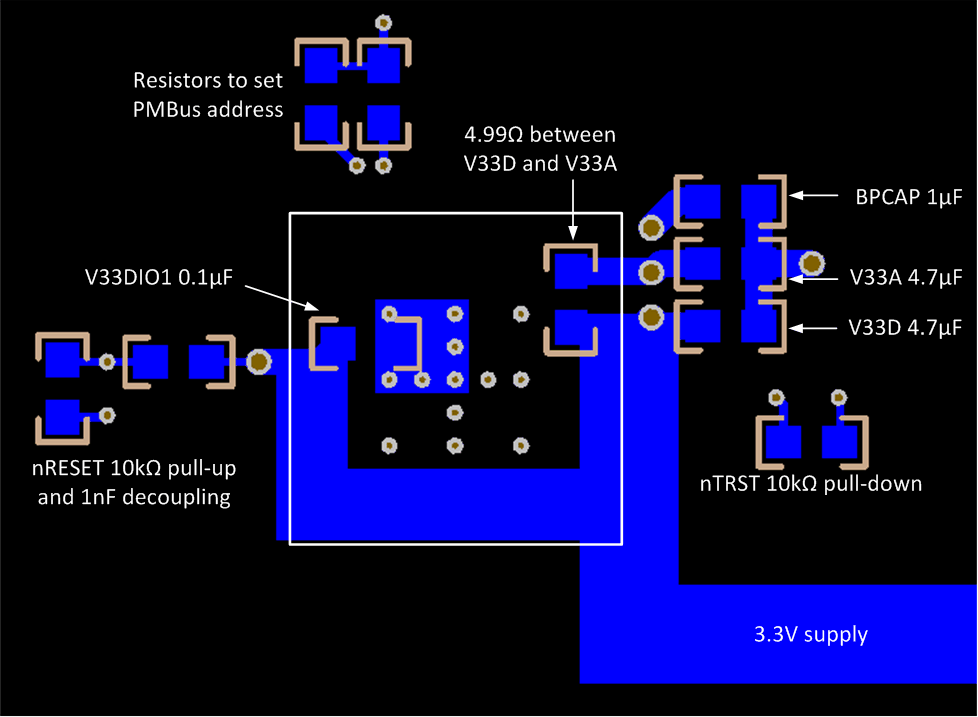
Layout Example

UCD90160A layout_01_slvsac8.gifFigure 35. Top Layer
UCD90160A layout_02_slvsac8.gifFigure 36. Bottom Layer