SLUSDC1 September 2018 UCD90320U
PRODUCTION DATA.
- 1 Features
- 2 Applications
- 3 Description
- 4 Revision History
- 5 Description Continued
- 6 Pin Configuration and Functions
- 7 Specifications
-
8 Detailed Description
- 8.1 Overview
- 8.2 Functional Block Diagram
- 8.3 Feature Description
- 8.4
Device Functional Modes
- 8.4.1 Rail Monitoring Configuration
- 8.4.2 GPI Configuration
- 8.4.3 Rail Sequence Configuration
- 8.4.4 Fault Responses Configuration
- 8.4.5 GPO Configuration
- 8.4.6 Margining Configuration
- 8.4.7 Pin Selected Rail States Configuration
- 8.4.8 Watchdog Timer
- 8.4.9 System Reset Function
- 8.4.10 Cascading Multiple Devices
- 8.4.11 Rail Monitoring
- 8.4.12 Status Monitoring
- 8.4.13 Data and Error Logging to EEPROM Memory
- 8.4.14 Black Box First Fault Logging
- 8.4.15 PMBus Address Selection
- 8.4.16 ADC Reference
- 8.4.17 Device Reset
- 8.4.18 Brownout
- 8.4.19 Internal Fault Management
- 8.4.20 Single Event Upset
- 8.5 Device Configuration and Programming
- 9 Application and Implementation
- 10Power Supply Recommendations
- 11Layout
- 12Device and Documentation Support
- 13Mechanical, Packaging, and Orderable Information
Package Options
Mechanical Data (Package|Pins)
- ZWS|169
Thermal pad, mechanical data (Package|Pins)
Orderable Information
8.4.10 Cascading Multiple Devices
Multiple UCD90320U devices can work together and coordinate to determine fault notification.
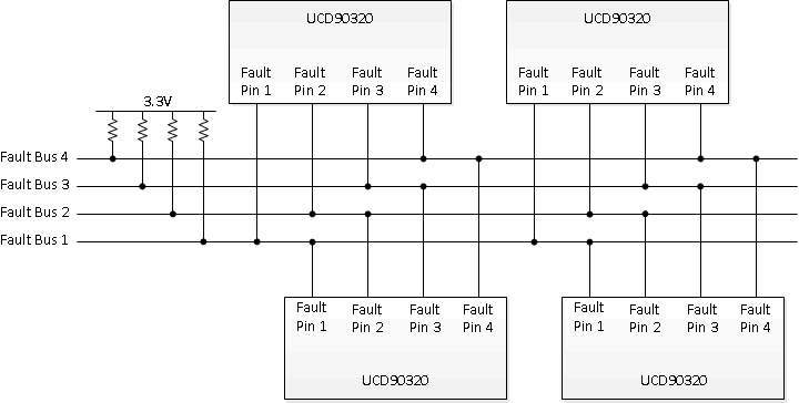
Up to 4 GPI pins can be configured as Fault Pins . Each Fault Pin is connected to a Fault Bus . Each Fault Bus is pulled up to 3.3 V by a 10-kΩ resistor. All the UCD90320U devices on the same Fault Bus are informed of the same fault condition. An example of Fault Pin connections is shown in Figure 28.
When there is no fault on a Fault Bus , the Fault Pins are digital input pins and listen to the Fault Bus . When one or multiple UCD90320U devices detect a rail fault, the corresponding Fault Pin is turned into active driven low state, pulling down the Fault Bus and informing all other UCD90320U devices of the corresponding fault. This way, a coordinated action can be taken across multiple devices. After the fault is cleared, the state of the Fault Pin is turned back to an input pin.
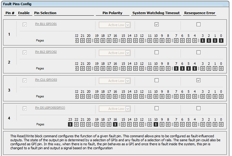
Any of the 24 rails can be assigned to one or multiple Fault Pins . The configuration window is shown in Figure 29.
 Figure 28. Example of Fault Pin Connections
  Figure 29. Example Fault Pins Configuration Window (Global Configuration ►Fault Pins Config)
 These listed page-related faults have impact on the fault pin output. SYSTEM_WATCHDOG_TIMEOUT and RESEQUENCE_ERROR are optional to have impact on the fault pins.
- IOUT_OC_FAULT
- IOUT_UC_FAULT
- OT_FAULT
- SEQ_OFF_TIMEOUT
- SEQ_ON_TIMEOUT
- TON_MAX_FAULT
- VOUT_OV_FAULT
- VOUT_UV_FAULT
A SYNC_CLK pin is used as a single-wire time synchronization method. A master chip constantly drives a 5-kHz clock to the slave devices. This function offers a precise time base for multiple UCD90320U devices to respond to the same fault event at the same time. The configuration window is shown in Figure 30. If the system uses only one UCD90320U device, it is recommended to configure this pin as master clock output. The SYNC_CLK output can be used as a time base for other purposes if needed.
 Figure 30. SYNC_CLK Pin Configuration (Global Configuration ► Misc Config)